JP2005509531A - Control of directional speed of chemical mechanical polishing pad conditioner to improve pad life - Google Patents
Control of directional speed of chemical mechanical polishing pad conditioner to improve pad life Download PDFInfo
- Publication number
- JP2005509531A JP2005509531A JP2003505115A JP2003505115A JP2005509531A JP 2005509531 A JP2005509531 A JP 2005509531A JP 2003505115 A JP2003505115 A JP 2003505115A JP 2003505115 A JP2003505115 A JP 2003505115A JP 2005509531 A JP2005509531 A JP 2005509531A
- Authority
- JP
- Japan
- Prior art keywords
- conditioning
- pad
- removal rate
- wafer
- material removal
- Prior art date
- Legal status (The legal status is an assumption and is not a legal conclusion. Google has not performed a legal analysis and makes no representation as to the accuracy of the status listed.)
- Pending
Links
Images


Classifications
-
- B—PERFORMING OPERATIONS; TRANSPORTING
- B24—GRINDING; POLISHING
- B24B—MACHINES, DEVICES, OR PROCESSES FOR GRINDING OR POLISHING; DRESSING OR CONDITIONING OF ABRADING SURFACES; FEEDING OF GRINDING, POLISHING, OR LAPPING AGENTS
- B24B37/00—Lapping machines or devices; Accessories
- B24B37/005—Control means for lapping machines or devices
- B24B37/013—Devices or means for detecting lapping completion
-
- B—PERFORMING OPERATIONS; TRANSPORTING
- B24—GRINDING; POLISHING
- B24B—MACHINES, DEVICES, OR PROCESSES FOR GRINDING OR POLISHING; DRESSING OR CONDITIONING OF ABRADING SURFACES; FEEDING OF GRINDING, POLISHING, OR LAPPING AGENTS
- B24B53/00—Devices or means for dressing or conditioning abrasive surfaces
- B24B53/017—Devices or means for dressing, cleaning or otherwise conditioning lapping tools
-
- B—PERFORMING OPERATIONS; TRANSPORTING
- B24—GRINDING; POLISHING
- B24B—MACHINES, DEVICES, OR PROCESSES FOR GRINDING OR POLISHING; DRESSING OR CONDITIONING OF ABRADING SURFACES; FEEDING OF GRINDING, POLISHING, OR LAPPING AGENTS
- B24B37/00—Lapping machines or devices; Accessories
- B24B37/005—Control means for lapping machines or devices
-
- B—PERFORMING OPERATIONS; TRANSPORTING
- B24—GRINDING; POLISHING
- B24B—MACHINES, DEVICES, OR PROCESSES FOR GRINDING OR POLISHING; DRESSING OR CONDITIONING OF ABRADING SURFACES; FEEDING OF GRINDING, POLISHING, OR LAPPING AGENTS
- B24B37/00—Lapping machines or devices; Accessories
- B24B37/04—Lapping machines or devices; Accessories designed for working plane surfaces
- B24B37/042—Lapping machines or devices; Accessories designed for working plane surfaces operating processes therefor
-
- B—PERFORMING OPERATIONS; TRANSPORTING
- B24—GRINDING; POLISHING
- B24B—MACHINES, DEVICES, OR PROCESSES FOR GRINDING OR POLISHING; DRESSING OR CONDITIONING OF ABRADING SURFACES; FEEDING OF GRINDING, POLISHING, OR LAPPING AGENTS
- B24B49/00—Measuring or gauging equipment for controlling the feed movement of the grinding tool or work; Arrangements of indicating or measuring equipment, e.g. for indicating the start of the grinding operation
- B24B49/02—Measuring or gauging equipment for controlling the feed movement of the grinding tool or work; Arrangements of indicating or measuring equipment, e.g. for indicating the start of the grinding operation according to the instantaneous size and required size of the workpiece acted upon, the measuring or gauging being continuous or intermittent
- B24B49/03—Measuring or gauging equipment for controlling the feed movement of the grinding tool or work; Arrangements of indicating or measuring equipment, e.g. for indicating the start of the grinding operation according to the instantaneous size and required size of the workpiece acted upon, the measuring or gauging being continuous or intermittent according to the final size of the previously ground workpiece
-
- B—PERFORMING OPERATIONS; TRANSPORTING
- B24—GRINDING; POLISHING
- B24B—MACHINES, DEVICES, OR PROCESSES FOR GRINDING OR POLISHING; DRESSING OR CONDITIONING OF ABRADING SURFACES; FEEDING OF GRINDING, POLISHING, OR LAPPING AGENTS
- B24B49/00—Measuring or gauging equipment for controlling the feed movement of the grinding tool or work; Arrangements of indicating or measuring equipment, e.g. for indicating the start of the grinding operation
- B24B49/18—Measuring or gauging equipment for controlling the feed movement of the grinding tool or work; Arrangements of indicating or measuring equipment, e.g. for indicating the start of the grinding operation taking regard of the presence of dressing tools
-
- G—PHYSICS
- G05—CONTROLLING; REGULATING
- G05B—CONTROL OR REGULATING SYSTEMS IN GENERAL; FUNCTIONAL ELEMENTS OF SUCH SYSTEMS; MONITORING OR TESTING ARRANGEMENTS FOR SUCH SYSTEMS OR ELEMENTS
- G05B19/00—Programme-control systems
-
- G—PHYSICS
- G05—CONTROLLING; REGULATING
- G05B—CONTROL OR REGULATING SYSTEMS IN GENERAL; FUNCTIONAL ELEMENTS OF SUCH SYSTEMS; MONITORING OR TESTING ARRANGEMENTS FOR SUCH SYSTEMS OR ELEMENTS
- G05B19/00—Programme-control systems
- G05B19/02—Programme-control systems electric
- G05B19/18—Numerical control [NC], i.e. automatically operating machines, in particular machine tools, e.g. in a manufacturing environment, so as to execute positioning, movement or co-ordinated operations by means of programme data in numerical form
- G05B19/19—Numerical control [NC], i.e. automatically operating machines, in particular machine tools, e.g. in a manufacturing environment, so as to execute positioning, movement or co-ordinated operations by means of programme data in numerical form characterised by positioning or contouring control systems, e.g. to control position from one programmed point to another or to control movement along a programmed continuous path
-
- G—PHYSICS
- G05—CONTROLLING; REGULATING
- G05B—CONTROL OR REGULATING SYSTEMS IN GENERAL; FUNCTIONAL ELEMENTS OF SUCH SYSTEMS; MONITORING OR TESTING ARRANGEMENTS FOR SUCH SYSTEMS OR ELEMENTS
- G05B19/00—Programme-control systems
- G05B19/02—Programme-control systems electric
- G05B19/418—Total factory control, i.e. centrally controlling a plurality of machines, e.g. direct or distributed numerical control [DNC], flexible manufacturing systems [FMS], integrated manufacturing systems [IMS] or computer integrated manufacturing [CIM]
- G05B19/41865—Total factory control, i.e. centrally controlling a plurality of machines, e.g. direct or distributed numerical control [DNC], flexible manufacturing systems [FMS], integrated manufacturing systems [IMS] or computer integrated manufacturing [CIM] characterised by job scheduling, process planning, material flow
-
- H—ELECTRICITY
- H01—ELECTRIC ELEMENTS
- H01L—SEMICONDUCTOR DEVICES NOT COVERED BY CLASS H10
- H01L21/00—Processes or apparatus adapted for the manufacture or treatment of semiconductor or solid state devices or of parts thereof
- H01L21/02—Manufacture or treatment of semiconductor devices or of parts thereof
- H01L21/04—Manufacture or treatment of semiconductor devices or of parts thereof the devices having potential barriers, e.g. a PN junction, depletion layer or carrier concentration layer
- H01L21/18—Manufacture or treatment of semiconductor devices or of parts thereof the devices having potential barriers, e.g. a PN junction, depletion layer or carrier concentration layer the devices having semiconductor bodies comprising elements of Group IV of the Periodic Table or AIIIBV compounds with or without impurities, e.g. doping materials
- H01L21/30—Treatment of semiconductor bodies using processes or apparatus not provided for in groups H01L21/20 - H01L21/26
- H01L21/302—Treatment of semiconductor bodies using processes or apparatus not provided for in groups H01L21/20 - H01L21/26 to change their surface-physical characteristics or shape, e.g. etching, polishing, cutting
- H01L21/304—Mechanical treatment, e.g. grinding, polishing, cutting
-
- H—ELECTRICITY
- H01—ELECTRIC ELEMENTS
- H01L—SEMICONDUCTOR DEVICES NOT COVERED BY CLASS H10
- H01L21/00—Processes or apparatus adapted for the manufacture or treatment of semiconductor or solid state devices or of parts thereof
- H01L21/67—Apparatus specially adapted for handling semiconductor or electric solid state devices during manufacture or treatment thereof; Apparatus specially adapted for handling wafers during manufacture or treatment of semiconductor or electric solid state devices or components ; Apparatus not specifically provided for elsewhere
- H01L21/67005—Apparatus not specifically provided for elsewhere
- H01L21/67242—Apparatus for monitoring, sorting or marking
- H01L21/67253—Process monitoring, e.g. flow or thickness monitoring
-
- H—ELECTRICITY
- H01—ELECTRIC ELEMENTS
- H01L—SEMICONDUCTOR DEVICES NOT COVERED BY CLASS H10
- H01L21/00—Processes or apparatus adapted for the manufacture or treatment of semiconductor or solid state devices or of parts thereof
- H01L21/67—Apparatus specially adapted for handling semiconductor or electric solid state devices during manufacture or treatment thereof; Apparatus specially adapted for handling wafers during manufacture or treatment of semiconductor or electric solid state devices or components ; Apparatus not specifically provided for elsewhere
- H01L21/67005—Apparatus not specifically provided for elsewhere
- H01L21/67242—Apparatus for monitoring, sorting or marking
- H01L21/67276—Production flow monitoring, e.g. for increasing throughput
-
- H—ELECTRICITY
- H01—ELECTRIC ELEMENTS
- H01L—SEMICONDUCTOR DEVICES NOT COVERED BY CLASS H10
- H01L22/00—Testing or measuring during manufacture or treatment; Reliability measurements, i.e. testing of parts without further processing to modify the parts as such; Structural arrangements therefor
- H01L22/20—Sequence of activities consisting of a plurality of measurements, corrections, marking or sorting steps
-
- G—PHYSICS
- G05—CONTROLLING; REGULATING
- G05B—CONTROL OR REGULATING SYSTEMS IN GENERAL; FUNCTIONAL ELEMENTS OF SUCH SYSTEMS; MONITORING OR TESTING ARRANGEMENTS FOR SUCH SYSTEMS OR ELEMENTS
- G05B2219/00—Program-control systems
- G05B2219/30—Nc systems
- G05B2219/32—Operator till task planning
- G05B2219/32053—Adjust work parameter as function of other cell
-
- G—PHYSICS
- G05—CONTROLLING; REGULATING
- G05B—CONTROL OR REGULATING SYSTEMS IN GENERAL; FUNCTIONAL ELEMENTS OF SUCH SYSTEMS; MONITORING OR TESTING ARRANGEMENTS FOR SUCH SYSTEMS OR ELEMENTS
- G05B2219/00—Program-control systems
- G05B2219/30—Nc systems
- G05B2219/32—Operator till task planning
- G05B2219/32065—Synchronise set points of processes
-
- G—PHYSICS
- G05—CONTROLLING; REGULATING
- G05B—CONTROL OR REGULATING SYSTEMS IN GENERAL; FUNCTIONAL ELEMENTS OF SUCH SYSTEMS; MONITORING OR TESTING ARRANGEMENTS FOR SUCH SYSTEMS OR ELEMENTS
- G05B2219/00—Program-control systems
- G05B2219/30—Nc systems
- G05B2219/45—Nc applications
- G05B2219/45031—Manufacturing semiconductor wafers
-
- H—ELECTRICITY
- H01—ELECTRIC ELEMENTS
- H01L—SEMICONDUCTOR DEVICES NOT COVERED BY CLASS H10
- H01L21/00—Processes or apparatus adapted for the manufacture or treatment of semiconductor or solid state devices or of parts thereof
- H01L21/02—Manufacture or treatment of semiconductor devices or of parts thereof
- H01L21/04—Manufacture or treatment of semiconductor devices or of parts thereof the devices having potential barriers, e.g. a PN junction, depletion layer or carrier concentration layer
- H01L21/18—Manufacture or treatment of semiconductor devices or of parts thereof the devices having potential barriers, e.g. a PN junction, depletion layer or carrier concentration layer the devices having semiconductor bodies comprising elements of Group IV of the Periodic Table or AIIIBV compounds with or without impurities, e.g. doping materials
- H01L21/30—Treatment of semiconductor bodies using processes or apparatus not provided for in groups H01L21/20 - H01L21/26
- H01L21/31—Treatment of semiconductor bodies using processes or apparatus not provided for in groups H01L21/20 - H01L21/26 to form insulating layers thereon, e.g. for masking or by using photolithographic techniques; After treatment of these layers; Selection of materials for these layers
- H01L21/3105—After-treatment
- H01L21/31051—Planarisation of the insulating layers
- H01L21/31053—Planarisation of the insulating layers involving a dielectric removal step
-
- Y—GENERAL TAGGING OF NEW TECHNOLOGICAL DEVELOPMENTS; GENERAL TAGGING OF CROSS-SECTIONAL TECHNOLOGIES SPANNING OVER SEVERAL SECTIONS OF THE IPC; TECHNICAL SUBJECTS COVERED BY FORMER USPC CROSS-REFERENCE ART COLLECTIONS [XRACs] AND DIGESTS
- Y02—TECHNOLOGIES OR APPLICATIONS FOR MITIGATION OR ADAPTATION AGAINST CLIMATE CHANGE
- Y02P—CLIMATE CHANGE MITIGATION TECHNOLOGIES IN THE PRODUCTION OR PROCESSING OF GOODS
- Y02P80/00—Climate change mitigation technologies for sector-wide applications
- Y02P80/40—Minimising material used in manufacturing processes
-
- Y—GENERAL TAGGING OF NEW TECHNOLOGICAL DEVELOPMENTS; GENERAL TAGGING OF CROSS-SECTIONAL TECHNOLOGIES SPANNING OVER SEVERAL SECTIONS OF THE IPC; TECHNICAL SUBJECTS COVERED BY FORMER USPC CROSS-REFERENCE ART COLLECTIONS [XRACs] AND DIGESTS
- Y02—TECHNOLOGIES OR APPLICATIONS FOR MITIGATION OR ADAPTATION AGAINST CLIMATE CHANGE
- Y02P—CLIMATE CHANGE MITIGATION TECHNOLOGIES IN THE PRODUCTION OR PROCESSING OF GOODS
- Y02P90/00—Enabling technologies with a potential contribution to greenhouse gas [GHG] emissions mitigation
- Y02P90/02—Total factory control, e.g. smart factories, flexible manufacturing systems [FMS] or integrated manufacturing systems [IMS]
Landscapes
- Engineering & Computer Science (AREA)
- Mechanical Engineering (AREA)
- Manufacturing & Machinery (AREA)
- General Physics & Mathematics (AREA)
- Physics & Mathematics (AREA)
- Automation & Control Theory (AREA)
- Microelectronics & Electronic Packaging (AREA)
- Power Engineering (AREA)
- Computer Hardware Design (AREA)
- Condensed Matter Physics & Semiconductors (AREA)
- Human Computer Interaction (AREA)
- General Engineering & Computer Science (AREA)
- Quality & Reliability (AREA)
- Mechanical Treatment Of Semiconductor (AREA)
- Finish Polishing, Edge Sharpening, And Grinding By Specific Grinding Devices (AREA)
- Grinding-Machine Dressing And Accessory Apparatuses (AREA)
Abstract
平坦化面をコンディショニングする方法、装置および媒体は、研磨パッド(102)およびコンディショニングディスク(108)を有する化学機械研磨(CMP)装置(100)の中に研磨するウェーハを取り付け、予め選択した最小および最大除去速度の範囲内にウェーハ材料除去速度が維持されるように選択した最初のパッドコンディショニングパラメータセットの下で、ウェーハを研磨し、研磨段階中のウェーハ材料除去速度を決定し、ウェーハ材料除去速度を最大および最小除去速度の範囲内に維持するように、更新されたパッドコンディショニングパラメータを計算し、更新されたコンディショニングパラメータを使用して研磨パッドをコンディショニングすることを含み、更新されたパッドコンディショニングパラメータは、コンディショニングディスクの回転速度および方向に基づいて研磨パッドのウェーハ材料除去速度を予測するパッド摩耗/コンディショニングモデルによって計算される。 A method, apparatus and medium for conditioning a planarized surface is provided by mounting a wafer to be polished in a chemical mechanical polishing (CMP) apparatus (100) having a polishing pad (102) and a conditioning disk (108), and a preselected minimum and Polish the wafer under the initial set of pad conditioning parameters selected to maintain the wafer material removal rate within the maximum removal rate range, determine the wafer material removal rate during the polishing phase, and determine the wafer material removal rate. Calculating updated pad conditioning parameters and conditioning the polishing pad using the updated conditioning parameters to maintain the value within the maximum and minimum removal rates, wherein the updated pad conditioning parameters are: , It is calculated by the pad wear / conditioning model that predicts the wafer material removal rate of the polishing pad based on the rotational speed and direction of the emission di partitioning disk.
Description
本発明は一般に研磨の分野を対象とし、研磨パッドの寿命および化学機械研磨プロセスにおける研磨パッドの有効性を向上させるための方法を対象とする。 The present invention is generally directed to the field of polishing and is directed to a method for improving the life of a polishing pad and the effectiveness of the polishing pad in a chemical mechanical polishing process.
本出願は、2001年6月19日出願の「Advanced Process Control for Semiconductor Manufacturing Process」という名称の出願第60/298878号、2001年7月16日出願の「Feedforward and Feedback Control for Conditioning of Chemical Mechanical Polishing Pad」という名称の出願第60/305798号、2001年9月12日出願の「Feedforward and Feedback Control for Conditioning of Chemical Mechanical Polishing Pad」という名称の出願第60/318743号、および2001年11月30日出願の「Control of Chemical Mechanical Polishing Pad Conditioner Directional Velocity to Improve Pad Life」という名称の出願第09/998,372号の優先権を主張するものである。これらはすべて参照によって本明細書に組み込まれる。 The present application is based on application No. 60/298878 filed Jun. 19, 2001, entitled “Advanced Process Control for Semiconductor Manufacturing Process”, and “Feedforward and Feedback Control for Conditioning of Chemical Mechanical Polishing” filed on Jul. 16, 2001. Application No. 60/305798, entitled “Pad”, Application No. 60/318743, entitled “Feedforward and Feedback Control for Conditioning of Chemical Mechanical Polishing Pad”, filed September 12, 2001, and November 30, 2001 The priority of the application No. 09 / 998,372 named “Control of Chemical Mechanical Polishing Pad Conditioner Directional Velocity to Improve Pad Life” is claimed. All of which are incorporated herein by reference.
化学機械研磨(chemical−mechanical polishing:CMP)は、半導体製造プロセスにおいて、半導体ウェーハ全面を平坦化するために使用される。この方法は、たとえばスラリで飽和した可動研磨パッドによる機械的接触および化学的腐食を使用して、ウェーハ(一般に二酸化シリコン(SiO2))から材料(たとえば表面犠牲材料層)を除去することを含む。高トポグラフィの領域(丘)は低トポグラフィの領域(谷)よりも速く除去されるので、研磨によって高低差がならされる。図1AにCMP機100の上面図を、図1Bに、線AAで切ったCMP機100の側断面図を示す。CMP機100には研磨対象のウェーハが供給される。一般に、CMP機100はアーム101でウェーハ105を持ち上げ、これを回転する研磨パッド102の上に置く。研磨パッド102は弾性材料から作られており、研磨プロセスを促進するためにしばしばテクスチャ(texture)が与えられている。研磨パッド102は、研磨パッド102の下に位置するプラテン104、すなわちターンテーブル上で所定の速度で回転する。ウェーハ105は、アーム101によって研磨パッド102上の適当な位置に保持される。ウェーハ105の下面は研磨パッド102の上に載っている。ウェーハ105の上面は、アーム101のウェーハキャリヤ106の下面と向き合っている。研磨パッド102が回転すると、アーム101はウェーハ105を所定の速度で回転させる。アーム101はウェーハ105を、所定のダウンフォース(down force)で研磨パッド102に対して押しつける。CMP機100はさらに、研磨パッド102の半径に沿って延びるスラリ分配アーム107を含む。スラリ分配アーム107は、研磨パッド102上にスラリ流を分配する。
Chemical-mechanical polishing (CMP) is used for planarizing the entire surface of a semiconductor wafer in a semiconductor manufacturing process. The method includes removing material (eg, a surface sacrificial material layer) from a wafer (typically silicon dioxide (SiO 2 )) using, for example, mechanical contact and chemical erosion with a movable polishing pad saturated with slurry. . Since the high topography region (hill) is removed faster than the low topography region (valley), the height difference is leveled by polishing. FIG. 1A shows a top view of the
時間が経つにつれて、研磨パッドはその粗さおよび弾性を失い、したがって所望の除去速度(研磨速度)を維持することができなくなる。所与の研磨パッドの材料除去速度は、図2に示すように、時間の経過とともに指数関数的に低下することが知られている。さらに、この除去速度の低下は、コンディショニングパラメータ、たとえばダウンフォースおよび/またはコンディショニング角速度および/またはコンディショニング時間を絶えず増大させて、ウェーハからの所望の材料除去速度を回復することを要求する。そのため、研磨サイクルと次の研磨サイクルの間に研磨パッドを(たとえばコンディショニングディスク108を使用して)コンディショニングしなければならない。コンディショニングディスクは、アーム109によって研磨パッド上の適当な位置に保持される。研磨パッドが回転するとコンディショニングディスク108も回転する。こうすることによってパッドの表面は粗くなり、少なくとも一時的に当初の材料除去速度を回復する。パッドの過度のコンディショニングはパッドの寿命を縮める。
Over time, the polishing pad loses its roughness and elasticity, and therefore cannot maintain the desired removal rate (polishing rate). It is known that the material removal rate for a given polishing pad decreases exponentially with time as shown in FIG. In addition, this reduction in removal rate requires that the conditioning parameters, such as downforce and / or conditioning angular velocity and / or conditioning time, be constantly increased to restore the desired material removal rate from the wafer. Therefore, the polishing pad must be conditioned (e.g., using conditioning disk 108) between the polishing cycle and the next polishing cycle. The conditioning disk is held in place on the polishing pad by
従来のコンディショニング法の問題は、研磨パッドがオーバーコンディショニングされる可能性、たとえばパッドがすり減ってしまう可能性があることである。ツールが必要な研磨を与えることを保証するために、パッドを交換するたびに1枚ないし数枚のウェーハを研磨し、その結果を測定しなければならない。これはそのまま処理の遅延およびツール効速度の低下につながる。 A problem with conventional conditioning methods is that the polishing pad can be overconditioned, for example, the pad can be worn out. One to several wafers must be polished and the results measured every time the pad is changed to ensure that the tool provides the necessary polishing. This directly leads to a delay in processing and a reduction in tool efficiency.
パッドの寿命を延ばす試みにおいては、研磨パッドの各部分を選択的にコンディショニングすること、または平坦化面上の廃棄材料の分布に基づいて、コンディショニング要素(たとえばコンディショニングディスク108)のダウンフォースをCMPパッドの表面に沿って変化させることができる。パッドの寿命を延ばす他の方法は、研磨パッドの不均一性に応答して、研磨パッドの表面全体のコンディショニング処方(recipe)を変化させることを含む。しかし、報告されているこれらのCMPプロセスは一般に、パッド寿命を延ばすことよりもCMPプロセスを改良すること、たとえばウォータ(water)の不均一性を改善することにより関心がある。 In an attempt to extend the life of the pad, the down-force of the conditioning element (e.g., conditioning disk 108) can be reduced by selectively conditioning each portion of the polishing pad or based on the distribution of waste material on the planarization surface. Can be varied along the surface. Other methods of extending the life of the pad include changing the conditioning recipe across the surface of the polishing pad in response to polishing pad non-uniformity. However, these reported CMP processes are generally more interested in improving the CMP process than extending pad life, eg, improving water non-uniformity.
パッドの寿命を延ばし、したがってパッド交換の頻度を小さくする方法および装置は、ウェーハ製造プロセスに大幅なコスト削減をもたらす。 Methods and apparatus that extend the life of the pad and thus reduce the frequency of pad replacement provide significant cost savings to the wafer manufacturing process.
本発明は、研磨パッドの平坦化面をコンディショニングしてパッドの実用寿命を延ばす方法、システムおよび媒体に関する。 The present invention relates to a method, system and medium for conditioning a planarized surface of a polishing pad to extend the useful life of the pad.
具体的には、本発明の少なくともいくつかの実施形態は、パッド摩耗/ウェーハ平坦化プロセスの物理および/または化学モデル(これは単一のモデルまたは複数のモデルとして実装することができる)を使用して、研磨パッドの性能を予測し、パッド寿命を延ばす。これによって、単一の研磨パッドで研磨することができる半導体ウェーハまたは他の基板の数が増大し、それによって、パッド寿命の延長およびパッド交換に充てる時間の短縮の両面においてCMPプロセスのコストがかなり削減される。 Specifically, at least some embodiments of the present invention use a physical and / or chemical model of the pad wear / wafer planarization process (which can be implemented as a single model or multiple models). Thus, the performance of the polishing pad is predicted and the life of the pad is extended. This increases the number of semiconductor wafers or other substrates that can be polished with a single polishing pad, thereby significantly increasing the cost of the CMP process, both in terms of extending pad life and reducing time spent on pad replacement. Reduced.
このモデルは、コンディショニングプロセスの「コンディショニング」動作パラメータに基づいて研磨の有効性(ウェーハ材料除去速度)を予測する。本発明の少なくともいくつかの実施形態では、コンディショニング動作パラメータが、コンディショニング中のコンディショニングディスク(ディスクを使用してコンディショニングする場合)の角方向および角速度を含み、さらに、コンディショニング頻度、コンディショニング時間などの他の因子を含むことができる。このモデルは、パッドをオーバーコンディショニングせず、許容されるウェーハ材料除去速度を提供する範囲の研磨パッドコンディショニングパラメータを選択し、これらのパラメータをこの範囲に維持する。したがって本発明は、CMP研磨プロセスのフィードフォワードおよびフィードバック制御のためのプロセスを提供する。 This model predicts polishing effectiveness (wafer material removal rate) based on the “conditioning” operating parameters of the conditioning process. In at least some embodiments of the invention, the conditioning operating parameters include the angular direction and angular velocity of the conditioning disk being conditioned (when using a disk for conditioning), and other conditions such as conditioning frequency, conditioning time, etc. Factors can be included. This model selects a range of polishing pad conditioning parameters that do not overcondition the pad and provides an acceptable wafer material removal rate, and maintains these parameters in this range. The present invention thus provides a process for feedforward and feedback control of a CMP polishing process.
本発明の一態様では、研磨パッドおよびコンディショニングディスクを有するCMP装置内で平坦化面をコンディショニングする方法は、CMP装置内で、予め選択した最小および最大除去速度の範囲内にウェーハ材料除去速度が維持されるように選択した最初のパッドコンディショニングパラメータセットの下で、ウェーハを研磨する段階と、前記研磨段階中のウェーハ材料除去速度を測定する段階と、前記ウェーハ材料除去速度に基づいて、ウェーハ材料除去速度を最大および最小除去速度の範囲内に維持するように、更新されたパッドコンディショニングパラメータを計算する段階と、更新されたコンディショニングパラメータを使用して研磨パッドをコンディショニングする段階とを含む。更新されたパッドコンディショニングパラメータは、パッド摩耗/パッド回復モデルを使用し、コンディショニングディスクの回転速度および方向を含むパッドコンディショニングパラメータの関数としてウェーハ材料除去速度を計算し、計算されたウェーハ材料除去速度と測定されたウェーハ材料除去速度との差を求め、前記差を低減する更新されたパッドコンディショニングパラメータを計算することによって計算される。更新されたパッドコンディショニングパラメータは、式k=(k1)+g×(k−(k1))に従って更新され、上式で、kは測定されたパラメータ、k1は計算されたパラメータの推定値、gは推定値ゲイン、(k−(k1))は予測誤差である。 In one aspect of the present invention, a method for conditioning a planarized surface in a CMP apparatus having a polishing pad and a conditioning disk maintains a wafer material removal rate within a preselected minimum and maximum removal rate within the CMP apparatus. Polishing a wafer under an initial set of pad conditioning parameters selected to be measured, measuring a wafer material removal rate during the polishing step, and removing the wafer material based on the wafer material removal rate Calculating updated pad conditioning parameters to condition the speed within the maximum and minimum removal rates; and conditioning the polishing pad using the updated conditioning parameters. The updated pad conditioning parameters use the pad wear / pad recovery model to calculate the wafer material removal rate as a function of the pad conditioning parameters including the rotational speed and direction of the conditioning disk, and the calculated wafer material removal rate and measurement And calculating updated pad conditioning parameters that reduce the difference. The updated pad conditioning parameters are updated according to the equation k = (k 1 ) + g × (k− (k 1 )), where k is the measured parameter and k 1 is the estimated parameter estimate. , G is an estimated value gain, and (k− (k 1 )) is a prediction error.
本発明の少なくともいくつかの実施形態では、最初のパッドコンディショニングパラメータセットが経験的に、または履歴データを使用して、あるいは実験計画(DOE)の結果を使用して決定される。 In at least some embodiments of the present invention, the initial pad conditioning parameter set is determined empirically, using historical data, or using experimental design (DOE) results.
本発明の少なくともいくつかの実施形態では、パッド摩耗/パッド回復モデルのパッドコンディショニングパラメータがさらに、コンディショニング頻度、またはコンディショニング時間、またはコンディショニング中のコンディショニングディスクの並進速度を含む。 In at least some embodiments of the present invention, the pad conditioning parameters of the pad wear / pad recovery model further include conditioning frequency, or conditioning time, or translation speed of the conditioning disk during conditioning.
本発明の少なくともいくつかの実施形態では、ウェーハ材料除去速度を決定する段階は、研磨の前後にウェーハの厚さを測定することを含む。 In at least some embodiments of the present invention, determining the wafer material removal rate includes measuring the thickness of the wafer before and after polishing.
本発明の少なくともいくつかの実施形態では、更新されたパッドコンディショニングパラメータを計算する段階(c)は、帰納的(recursive)最適化プロセスを実行することを含み、または少なくともいくつかの実施形態では、パラメータが決定された最小および最大値の範囲内となるようにコンディショニングパラメータを計算することを含む。 In at least some embodiments of the invention, the step (c) of calculating the updated pad conditioning parameters comprises performing a recursive optimization process, or in at least some embodiments, Calculating the conditioning parameters such that the parameters are within the determined minimum and maximum values.
本発明の少なくともいくつかの実施形態では、ゲインは、測定されたパラメータの変動性または信頼性の指標であり、ゲインは約0.5から1.0、または約0.7から0.9の範囲にある。 In at least some embodiments of the present invention, the gain is a measure of the variability or reliability of the measured parameter, and the gain is about 0.5 to 1.0, or about 0.7 to 0.9. Is in range.
少なくともいくつかの実施形態では、更新されたパッドコンディショニングパラメータは、パッド摩耗/パッドコンディショニングモデルの出力とウェーハ材料除去段階(c)との間の差を求めることによって計算される。少なくともいくつかの実施形態では、この差は最小化される。 In at least some embodiments, the updated pad conditioning parameters are calculated by determining the difference between the pad wear / pad conditioning model output and the wafer material removal step (c). In at least some embodiments, this difference is minimized.
本発明の少なくともいくつかの実施形態では、段階(b)から(e)までを繰り返す。 In at least some embodiments of the invention, steps (b) through (e) are repeated.
本発明の少なくともいくつかの実施形態では、ウェーハ材料除去速度の最大値は、ウェーハ材料除去速度対コンディショニングダウンフォース曲線の飽和点であり、または少なくともいくつかの実施形態では、ウェーハ材料除去速度の最大値は初期除去速度であり、または少なくともいくつかの実施形態では、ウェーハ材料除去速度の最小値は、最大許容ウェーハ研磨時間によって定義される。 In at least some embodiments of the invention, the maximum wafer material removal rate is the saturation point of the wafer material removal rate versus the conditioning downforce curve, or in at least some embodiments, the maximum wafer material removal rate. The value is the initial removal rate, or in at least some embodiments, the minimum value for the wafer material removal rate is defined by the maximum allowable wafer polishing time.
本発明の少なくともいくつかの実施形態では、ウェーハ材料除去速度は下式によって定義され、 In at least some embodiments of the invention, the wafer material removal rate is defined by:
![]()
![]()
上式で、ωdiskは、研磨パッドのコンディショニング中のコンディショニングディスクの角速度、tはコンディショニング時間、fはコンディショニング頻度、directionは、コンディショニングディスクの回転方向、T2は、コンディショニング中のコンディショニングディスクの掃引速度である。 Where ω disk is the angular speed of the conditioning disk during conditioning of the polishing pad, t is the conditioning time, f is the conditioning frequency, direction is the direction of rotation of the conditioning disk, and T 2 is the sweep speed of the conditioning disk during conditioning. It is.
本発明の他の態様では、基板を平坦化するのに使用する研磨パッドをコンディショニングするための装置は、研磨パッドの平坦化面の上に配置可能なアームを有するキャリヤアセンブリと、キャリヤアセンブリに取り付けられたコンディショニングディスクと、コンディショニングディスクの動作パラメータを制御することができるアクチュエータと、アクチュエータに動作可能に結合されたコントローラであって、アクチュエータを操作して、コンディショニングディスクの動作パラメータを、コンディショニングパッドの回転速度および方向に基づいてウェーハ材料除去速度を予測するパッド摩耗/パッド回復モデルの関数として調整するコントローラとを備える。 In another aspect of the invention, an apparatus for conditioning a polishing pad used to planarize a substrate includes a carrier assembly having an arm that can be disposed on a planarizing surface of the polishing pad, and attached to the carrier assembly. A conditioning disk, an actuator capable of controlling the operating parameters of the conditioning disk, and a controller operably coupled to the actuator, wherein the actuator is operated to change the operating parameters of the conditioning disk and the rotation of the conditioning pad. A controller that adjusts as a function of a pad wear / pad recovery model that predicts wafer material removal rate based on velocity and direction.
本発明の少なくともいくつかの実施形態では、更新されたパッドコンディショニングパラメータは、パッド摩耗/パッド回復モデルを使用し、コンディショニングディスクの回転速度および方向を含むパッドコンディショニングパラメータの関数としてウェーハ材料除去速度を計算し、計算されたウェーハ材料除去速度と測定されたウェーハ材料除去速度との差を求め、前記差を低減する更新されたパッドコンディショニングパラメータを計算することによって計算される。更新されたパッドコンディショニングパラメータは、式k=(k1)+g×(k−(k1))に従って更新され、上式で、kは測定されたパラメータ、k1は計算されたパラメータの推定値、gは推定値ゲイン、(k−(k1))は予測誤差である。 In at least some embodiments of the present invention, the updated pad conditioning parameters use a pad wear / pad recovery model to calculate wafer material removal rates as a function of pad conditioning parameters including conditioning disk rotation speed and direction. Calculating a difference between the calculated wafer material removal rate and the measured wafer material removal rate, and calculating an updated pad conditioning parameter that reduces the difference. The updated pad conditioning parameters are updated according to the equation k = (k 1 ) + g × (k− (k 1 )), where k is the measured parameter and k 1 is the estimated parameter estimate. , G is an estimated value gain, and (k− (k 1 )) is a prediction error.
少なくともいくつかの実施形態では、パッド摩耗/パッド回復モデルのパッドコンディショニングパラメータがさらに、コンディショニング頻度、またはコンディショニング時間、またはコンディショニング中のコンディショニングディスクの速度を含む。 In at least some embodiments, the pad conditioning parameters of the pad wear / pad recovery model further include conditioning frequency, or conditioning time, or conditioning disk speed during conditioning.
本発明の少なくともいくつかの実施形態では、ゲインは、測定されたパラメータの変動性または信頼性の指標である。 In at least some embodiments of the invention, the gain is a measure of the variability or reliability of the measured parameter.
本発明の他の態様では、ウェーハから材料を除去するのに使用する研磨パッドのパッドコンディショニングを最適化するためのパッド摩耗/パッドコンディショニングモデルを開発する方法が提供される。この方法は、
a)少なくとも1つのパッドコンディショニングパラメータとウェーハ材料除去速度の間の関係を決定する段階と、
b)少なくとも1つのパッドコンディショニングパラメータおよびウェーハ材料除去速度について、それぞれに最大値および最小値を決定する段階と、
c)少なくとも1つのパッドコンディショニングパラメータとウェーハ除去速度の関係、ならびに少なくとも1つのパッドコンディショニングパラメータおよびウェーハ除去速度の最小および最大値を記録する段階と
を含む。
In another aspect of the invention, a method is provided for developing a pad wear / pad conditioning model for optimizing the pad conditioning of a polishing pad used to remove material from a wafer. This method
a) determining a relationship between at least one pad conditioning parameter and a wafer material removal rate;
b) determining a maximum value and a minimum value, respectively, for at least one pad conditioning parameter and wafer material removal rate;
c) recording the relationship between the at least one pad conditioning parameter and the wafer removal rate, and the minimum and maximum values of the at least one pad conditioning parameter and the wafer removal rate.
本発明の少なくともいくつかの実施形態では、少なくとも1つのパッドコンディショニングパラメータは複数のパラメータを含み、ウェーハ除去速度は、複数のパッドコンディショニングパラメータの重み付き関数として定義され、
または少なくともいくつかの実施形態では、少なくとも1つのパッドコンディショニングパラメータはコンディショニングディスクの回転速度を含み、
または少なくともいくつかの実施形態では、少なくとも1つのパッドコンディショニングパラメータはコンディショニングディスクの回転方向を含む。
In at least some embodiments of the invention, the at least one pad conditioning parameter includes a plurality of parameters, and the wafer removal rate is defined as a weighted function of the plurality of pad conditioning parameters;
Or in at least some embodiments, the at least one pad conditioning parameter comprises the rotational speed of the conditioning disk;
Or, in at least some embodiments, the at least one pad conditioning parameter includes the direction of rotation of the conditioning disk.
本発明の少なくともいくつかの実施形態では、少なくとも1つのパッドコンディショニングパラメータは、コンディショニングディスクのダウンフォース、コンディショニングディスクの回転速度および方向、コンディショニング頻度および継続時間、ならびにコンディショニングディスクの並進速度からなるグループから選択された1つまたは複数のパラメータを含む。 In at least some embodiments of the invention, the at least one pad conditioning parameter is selected from the group consisting of conditioning disk downforce, conditioning disk rotation speed and direction, conditioning frequency and duration, and conditioning disk translation speed. One or more parameters.
本発明の少なくともいくつかの実施形態では、少なくとも1つのコンディショニングパラメータとウェーハ除去速度との間の関係は、コンディショニングパラメータを段階的に変化させ、その結果生じたウェーハ除去速度を測定することによって決定される。 In at least some embodiments of the invention, the relationship between the at least one conditioning parameter and the wafer removal rate is determined by stepping the conditioning parameter and measuring the resulting wafer removal rate. The
本発明の少なくともいくつかの実施形態では、コンディショニングパラメータの最大値は、ウェーハ除去速度の段階的な増大が観察されない値であり、または少なくともいくつかの実施形態では、コンディショニングパラメータの最小値は、最低限のウェーハ除去速度を与える値である。 In at least some embodiments of the invention, the maximum value of the conditioning parameter is a value at which no step increase in wafer removal rate is observed, or in at least some embodiments, the minimum value of the conditioning parameter is the lowest It is a value that gives a limited wafer removal rate.
本発明の少なくともいくつかの実施形態では、本発明はさらに、CMP装置内で、予め選択した最小および最大除去速度の範囲内にウェーハ材料除去速度が維持されるように選択した、コンディショニングディスクの回転速度および方向を含む最初のパッドコンディショニングパラメータセットの下で、ウェーハを研磨する段階と、前記研磨段階中のウェーハ材料除去速度を決定する段階と、決定されたウェーハ材料除去速度およびパッド摩耗/コンディショニングモデルに基づいて、ウェーハ材料除去速度を最大および最小除去速度の範囲内に維持するように、更新されたパッドコンディショニングパラメータを計算する段階と、更新されたコンディショニングパラメータを使用して研磨パッドをコンディショニングする段階とを含む。 In at least some embodiments of the present invention, the present invention further includes rotating a conditioning disk selected within the CMP apparatus to maintain the wafer material removal rate within a preselected minimum and maximum removal rate range. Polishing a wafer under a first set of pad conditioning parameters including speed and direction; determining a wafer material removal rate during said polishing step; and determined wafer material removal rate and pad wear / conditioning model And calculating updated pad conditioning parameters to condition the wafer material removal rate within the maximum and minimum removal rates, and conditioning the polishing pad using the updated conditioning parameters Including.
本発明の少なくともいくつかの実施形態では、更新されたパッドコンディショニングパラメータは、パッド摩耗/コンディショニングモデルの出力と決定されたウェーハ材料除去との間の差を求めることによって計算され、または少なくともいくつかの実施形態では、更新されたパッドコンディショニングパラメータは、式k=(k−1)+g×(k−(k−1))に従って更新され、上式で、kは測定されたウェーハ材料除去速度、k1は計算されたウェーハ材料除去速度、gは推定値ゲイン、(k−(k1))は予測誤差である。 In at least some embodiments of the present invention, the updated pad conditioning parameters are calculated by determining a difference between the output of the pad wear / conditioning model and the determined wafer material removal, or at least some In an embodiment, the updated pad conditioning parameters are updated according to the equation k = (k−1) + g × (k− (k−1)), where k is the measured wafer material removal rate, k1 Is the calculated wafer material removal rate, g is the estimated value gain, and (k− (k1)) is the prediction error.
本発明の他の態様では、コンピュータによって実行される命令を有し、この命令が、化学機械研磨プロセスのためのコンピュータ実装ソフトウェアアプリケーションを含むコンピュータ可読媒体が提供される。このプロセスを実装するための命令は、
a)化学機械研磨プロセスで処理された少なくとも1枚のウェーハのウェーハ除去速度に関するデータを化学機械研磨ツールから受け取ること、ならびに
b)段階(a)のデータから、定義された最大および最小値の範囲内の更新されたパッドコンディショニングパラメータを、パッド摩耗/コンディショニングモデルの出力と段階(a)のデータとの間の差を求めることによって計算すること
を含む。
In another aspect of the invention, there is provided a computer readable medium having instructions executed by a computer, the instructions including a computer implemented software application for a chemical mechanical polishing process. The instructions to implement this process are
a) receiving from the chemical mechanical polishing tool data regarding the wafer removal rate of at least one wafer processed in the chemical mechanical polishing process; and b) a range of defined maximum and minimum values from the data of step (a). And calculating updated pad conditioning parameters by determining the difference between the pad wear / conditioning model output and the data of step (a).
本発明の少なくともいくつかの実施形態では、更新されたコンディショニングパラメータを計算することは、パラメータが決定された最小および最大値の範囲内となるようにパラメータを計算することを含み、または少なくともいくつかの実施形態では、段階(b)の更新されたパッドコンディショニングパラメータを計算することは、帰納的最適化プロセスを実行することを含む。 In at least some embodiments of the invention, calculating the updated conditioning parameters includes calculating the parameters such that the parameters are within the determined minimum and maximum values, or at least some In this embodiment, calculating the updated pad conditioning parameters of step (b) includes performing an inductive optimization process.
本発明の少なくともいくつかの実施形態では、ウェーハ材料除去速度の最大値は、ウェーハ材料除去速度対コンディショニングダウンフォース曲線の飽和点であり、または少なくともいくつかの実施形態では、ウェーハ材料除去速度の最大値は初期除去速度であり、または少なくともいくつかの実施形態では、ウェーハ材料除去速度の最小値は、最小許容ウェーハ研磨時間によって定義される。 In at least some embodiments of the present invention, the maximum wafer material removal rate is the saturation point of the wafer material removal rate versus the conditioning downforce curve, or in at least some embodiments, the maximum wafer material removal rate. The value is the initial removal rate, or in at least some embodiments, the minimum value for the wafer material removal rate is defined by the minimum allowable wafer polishing time.
本発明の少なくともいくつかの実施形態では、更新されたコンディショニングパラメータを計算する前に、推定値ゲインを使用して前記差を調整する。 In at least some embodiments of the present invention, the estimated gain is used to adjust the difference before calculating the updated conditioning parameters.
本発明の他の態様では、研磨パッドを有し、研磨パッドに対して、ウェーハから材料を除去するためにウェーハが配置され、研磨パッドをコンディショニングするためにコンディショニングディスクが配置された化学機械研磨(CMP)装置内で平坦化面をコンディショニングする方法が提供される。この方法は、
(a)
(i)少なくとも1つのパッドコンディショニングパラメータとウェーハ材料除去速度の間の関係を決定し、
(ii)少なくとも1つのパッドコンディショニングパラメータおよびウェーハ材料除去速度について、それぞれに最大値および最小値を決定し、
(iii)少なくとも1つのパッドコンディショニングパラメータとウェーハ除去速度の関係、ならびに少なくとも1つのパッドコンディショニングパラメータおよびウェーハ除去速度の最小および最大値を記録する
ことによって、ウェーハ材料除去速度をパッドコンディショニングパラメータの関数として定義するパッド摩耗/パッドコンディショニングモデルを開発する段階と、
(b)CMP装置内で、予め選択した最小および最大除去速度の範囲内にウェーハ材料除去速度が維持されるように選択した、コンディショニングディスクの回転速度および方向を含む最初のパッドコンディショニングパラメータセットの下で、ウェーハを研磨する段階と、
(c)前記研磨段階中のウェーハ材料除去速度を決定する段階と、
(d)段階(b)の決定されたウェーハ材料除去速度およびパッド摩耗/コンディショニングモデルに基づいて、ウェーハ材料除去速度を最大および最小除去速度の範囲内に維持するように、更新されたパッドコンディショニングパラメータを計算する段階と、
(f)更新されたコンディショニングパラメータを使用して研磨パッドをコンディショニングする段階と
を含む。
In another aspect of the invention, a chemical mechanical polishing having a polishing pad, wherein the wafer is positioned to remove material from the wafer and a conditioning disk is positioned to condition the polishing pad. A method for conditioning a planarized surface in a CMP) apparatus is provided. This method
(A)
(I) determining a relationship between at least one pad conditioning parameter and a wafer material removal rate;
(Ii) determining a maximum value and a minimum value for each of at least one pad conditioning parameter and wafer material removal rate;
(Iii) Define wafer material removal rate as a function of pad conditioning parameters by recording the relationship between at least one pad conditioning parameter and wafer removal rate, and the minimum and maximum values of at least one pad conditioning parameter and wafer removal rate. Developing a pad wear / pad conditioning model to perform,
(B) Under the initial pad conditioning parameter set, including the rotational speed and direction of the conditioning disk, selected to maintain the wafer material removal rate within a preselected range of minimum and maximum removal rates within the CMP apparatus. And polishing the wafer,
(C) determining a wafer material removal rate during the polishing step;
(D) updated pad conditioning parameters to maintain the wafer material removal rate within the maximum and minimum removal rates based on the determined wafer material removal rate and pad wear / conditioning model of step (b). A step of calculating
(F) conditioning the polishing pad using the updated conditioning parameters.
本発明の他の態様では、研磨パッドを有し、研磨パッドに対して、ウェーハから材料を除去するためにウェーハが配置され、研磨パッドをコンディショニングするためにコンディショニングディスクが配置された化学機械研磨(CMP)装置内で平坦化面をコンディショニングするためのシステムは、
a)コンディショニングディスクの回転および方向を含む少なくとも1つのパッドコンディショニングパラメータの関数としてウェーハ材料除去速度を定義するパッド摩耗/コンディショニングモデルと、
b)CMP装置内でウェーハを研磨する研磨手段と、
c)ウェーハ材料除去速度を決定するための測定手段と、
d)段階(c)の手段を使用して測定されたウェーハ材料除去速度およびパッド摩耗/コンディショニングモデルに基づいて、ウェーハ材料除去速度を最大および最小除去速度の範囲内に維持するためにパッドコンディショニングパラメータを更新するための計算手段と
を備える。
In another aspect of the invention, a chemical mechanical polishing having a polishing pad, wherein the wafer is positioned to remove material from the wafer and a conditioning disk is positioned to condition the polishing pad. A system for conditioning a planarized surface in a CMP) apparatus is:
a) a pad wear / conditioning model that defines wafer material removal rate as a function of at least one pad conditioning parameter including rotation and direction of the conditioning disk;
b) a polishing means for polishing the wafer in the CMP apparatus;
c) measuring means for determining the wafer material removal rate;
d) Pad conditioning parameters to maintain the wafer material removal rate within the maximum and minimum removal rates based on the wafer material removal rate and pad wear / conditioning model measured using the means of step (c). And a calculation means for updating.
このように、適当なコンディショニング角速度を使用してウェーハ材料除去速度を許容範囲内に維持し、除去速度が許容される除去速度よりも低くなるたびにコンディショニングの方向を逆転させ、かつ/あるいは角速度または他のコンディショニングパラメータを調整することによって、研磨パッド寿命は延長される。「万能サイズ(one size fits all)」手法をパッドコンディショニングパラメータに適用することによって、たとえば、実際のウェーハ材料除去速度の変化を考慮することなくコンディショニングパラメータを決定することによって、従来のプロセスは過剰に補償し、それによってパッド材料を必要以上に除去し、パッドの摩耗を加速させる。対照的に本発明は、損傷したパッドを再コンディショニングするのに最低限必要な力を求めることによって、改良されたコンディショニングパラメータを提供する。 In this way, an appropriate conditioning angular velocity is used to maintain the wafer material removal rate within an acceptable range, reversing the direction of conditioning each time the removal rate is lower than the acceptable removal rate, and / or the angular velocity or By adjusting other conditioning parameters, the polishing pad life is extended. By applying the “one size fits all” approach to the pad conditioning parameters, for example, by determining the conditioning parameters without taking into account changes in the actual wafer material removal rate, Compensate, thereby removing more pad material than necessary and accelerating pad wear. In contrast, the present invention provides improved conditioning parameters by determining the minimum force required to recondition a damaged pad.
本発明のさまざまな目的、特徴および利点は、本発明の以下の詳細な説明を図面とともに検討したときにより完全に理解することができる。 Various objects, features and advantages of the present invention can be more fully understood when the following detailed description of the invention is considered in conjunction with the drawings.
次に、研磨パッドの寿命を最大にするためのCMPプロセスの新規のフィードフォワードおよびフィードバック法を説明する。パッドの寿命が延びると、交換または調整(たとえばパッドの損傷部分の除去)の必要なしにより長い期間にわたってより多くのウェーハを研磨できるので、CMPプロセスのダウンタイム(down time)が短縮する。用語ウェーハは一般的な意味で使用され、研磨を受ける実質的に平らな任意の物体を含む。ウェーハは、モノリス構造の他に、1つまたは複数の層を有する基層、あるいはその上に付着された薄膜または他の構造を含む。 Next, a novel feedforward and feedback method of the CMP process to maximize the life of the polishing pad is described. Extended pad life reduces CMP process down time because more wafers can be polished over longer periods without the need for replacement or adjustment (eg, removal of damaged portions of the pad). The term wafer is used in a general sense and includes any substantially flat object that undergoes polishing. In addition to the monolith structure, the wafer includes a base layer having one or more layers, or a thin film or other structure deposited thereon.
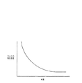
CMPプロセスに必要なウェーハ材料除去速度を提供するため、研磨パッドの表面は、その粗さおよび弾性をある水準に維持する必要がある。パッドの粗さおよび弾性はウェーハを研磨し続けるうちに低下し、これによってウェーハ材料除去速度は低減する。研磨パッドの初期の表面状態(突起320)を図3Aに示す。このとき、表面粗さは最大となっている。パッドを研磨に使用した後は、これらの突起がしばしばさまざまな方向に押し倒されている。これを補償し、パッドの粗さの少なくとも一部を回復するため、このパッドをたとえば、たとえば図3Bに示す矢印340が指示する方向に回転するコンディショニングディスクを使用してコンディショニングする。本明細書ではディスク型のコンディショナを用いて本発明を説明するが、他のコンディショニング機構の使用も明確に企図される。しかしこれによって、パッドの表面特徴320に方向バイアスが導入される。以降のコンディショニング操作を同じコンディショニング方向を使用して実施すると、パッド表面の突起の方向性が増し、これによってパッド中でのスラリの流れが妨げられ、さらに、パッドの突起と研磨中のウェーハとの間の接触面が小さくなる可能性がある。これが、よりいっそう大きな方向バイアスが導入された図3Cの突起320に示されている。その結果、パッド表面特徴の方向バイアスが増大するにつれてウェーハ材料除去速度は悪化する。図2には、図3A〜Cに示したコンディショニングプロセスの結果である、時間の経過に伴う除去速度の低下が示されている。
In order to provide the necessary wafer material removal rate for the CMP process, the surface of the polishing pad needs to maintain its roughness and elasticity at some level. The roughness and elasticity of the pad decreases as the wafer continues to be polished, thereby reducing the wafer material removal rate. The initial surface state (protrusion 320) of the polishing pad is shown in FIG. 3A. At this time, the surface roughness is maximum. These protrusions are often pushed down in various directions after the pad is used for polishing. To compensate for this and restore at least a portion of the pad roughness, the pad is conditioned, for example, using a conditioning disk that rotates in the direction indicated by
図4A、4Bおよび4Cは、上述の方向バイアスの問題を解決する目的に使用される、単純化されたモデルを表す。このモデルでは、コンディショニングディスクの角速度が交番する。最初に図4Aを参照する。この図は研磨パッドの初期表面状態を示している。研磨パッド400をコンディショニングディスクと最初の角速度で(たとえば図4Bの矢印420によって指示される時計回りに)接触させることによって、研磨パッド400をコンディショニングする。これによって、研磨パッドの表面特徴440にある方向性が導入される。続くコンディショニング事象で、コンディショニングディスクの角速度を(たとえば図4Cの矢印460によって示される反時計回りに)逆転させて、以前のコンディショニング事象の影響を「除去」する。コンディショニングの速度および方向を交番させると、表面粗さおよび弾性が持続する。図4A、4Bおよび4Cに示すプロセスは、パッドのライフサイクル全体にわたって、使用可能な活性部位がなくなるまで繰り返すことができる。
4A, 4B, and 4C represent a simplified model that is used to solve the directional bias problem described above. In this model, the angular velocity of the conditioning disk alternates. Reference is first made to FIG. 4A. This figure shows the initial surface state of the polishing pad. The
したがって、研磨パッドを最初の方向に所定の回数にわたってコンディショニングし、その後にコンディショニング方向を逆転させることができる。特定の方向へのコンディショニング事象の最適回数は、パッドが古くなるにつれて変化する(減少する)と予想される。このパッドコンディショニング/回復モデルはそれに応じてプロセスを調整する。 Accordingly, the polishing pad can be conditioned in the initial direction for a predetermined number of times, after which the conditioning direction can be reversed. The optimal number of conditioning events in a particular direction is expected to change (decrease) as the pad ages. This pad conditioning / recovery model adjusts the process accordingly.
研磨パッドによるウェーハの平坦化およびコンディショニング中の上述の機械的プロセスは、平坦化プロセスを最適化するためのモデルを提供する。このモデルに従ってパッドコンディショニングパラメータを調整することによって、ウェーハ材料除去速度を犠牲にすることなく、パッドの寿命を延ばすことができる。具体的には、コンディショニングディスクの速度および方向、ならびに任意選択の他の動作変数、たとえばコンディショニング頻度、コンディショニング継続時間、コンディショニングディスクのパッド表面での移動速度を、パッドのコンディショニングの動作パラメータを予測し次いでこれらを最適化するフィードバックおよびフィードフォワードループで調整する。 The mechanical processes described above during wafer planarization and conditioning with a polishing pad provide a model for optimizing the planarization process. By adjusting the pad conditioning parameters according to this model, the life of the pad can be extended without sacrificing the wafer material removal rate. Specifically, the conditioning disk speed and direction, as well as other optional operating variables such as conditioning frequency, conditioning duration, speed of movement of the conditioning disk on the pad surface, predict the operating parameters of the pad conditioning, and Adjust these with feedback and feed-forward loops to optimize them.
本発明の少なくともいくつかの実施形態によれば、ウェーハ研磨プロセスの知識に基づいて初期モデルを開発し、これを、本発明の少なくともいくつかの実施形態において、図5に示すように使用する。初期モデル、たとえばウェーハおよび研磨パッドパラメータが一定である初期モデルに基づいて、所与のコンディショニングパラメータセットの予め選択された最小値と最大値の間に含まれるウェーハ材料除去速度を提供する初期処理条件を識別する。以下、この最小値と最大値の間の範囲をウェーハ材料除去速度の「許容可能」範囲と呼ぶ。これらの条件は、パッドのオーバーコンディショニングが起こらないように選択される。 In accordance with at least some embodiments of the present invention, an initial model is developed based on knowledge of the wafer polishing process and used in at least some embodiments of the present invention as shown in FIG. Initial processing conditions that provide a wafer material removal rate that falls between preselected minimum and maximum values for a given set of conditioning parameters based on an initial model, for example, an initial model where the wafer and polishing pad parameters are constant Identify Hereinafter, the range between the minimum and maximum values is referred to as the “acceptable” range of the wafer material removal rate. These conditions are selected so that pad overconditioning does not occur.
次に図5を参照する。段階500で、この初期条件に従ってウェーハを研磨する。段階510で、研磨したウェーハの厚さを測定し、ウェーハ材料除去速度を計算する。この情報は後に、フィードバックループで、ウェーハ材料除去速度を許容範囲内に維持するのに使用される。この実際の除去速度を(パッド摩耗モデルから導かれた)予測除去速度と比較する。偏差、すなわち予測誤差を使用して、段階520で、このモデルで識別された研磨パッドの研磨能力の低下を補償し、かつ/またはモデル化されていない任意の効果を補正する本発明のモデルに従って、パッドコンディショニングパラメータを調整する。更新されたコンディショニングパラメータに従って、段階530で、研磨パッドをコンディショニングする。段階540で研磨を繰り返し、その研磨結果を使用し、段階510〜530を繰り返すことによって研磨条件をさらに更新する。
Reference is now made to FIG. In
ウェーハ材料除去速度およびコンディショニングパラメータを、予め選択した最小〜最大範囲内に維持することによって、パッドのオーバーコンディショニングが防止される。すなわち、研磨パッドの有効性を回復させるのには十分だが、パッドを必要以上に傷つけないコンディショニングパラメータを使用することができる。動作時には、最小許容除去速度に近いウェーハ材料除去速度が得られるパッドコンディショニングパラメータを選択することが望ましい場合がある。最小許容限度に近いコンディショニング力はあまり攻撃的でなく、したがってこれによって研磨パッドのオーバーコンディショニングが回避される確度が高まるからである。しかし、パッド状態の突然の劣化によって、ウェーハ材料除去速度が最小許容速度よりも低くなる可能性があるので、最小材料除去速度に近づけ過ぎた条件で操作することについては用心深く(または少なくとも認識してい)なければならない。 By maintaining the wafer material removal rate and conditioning parameters within a preselected minimum to maximum range, pad overconditioning is prevented. That is, conditioning parameters can be used that are sufficient to restore the effectiveness of the polishing pad, but do not damage the pad more than necessary. In operation, it may be desirable to select pad conditioning parameters that result in a wafer material removal rate close to the minimum allowable removal rate. Conditioning forces close to the minimum acceptable limit are not very aggressive and therefore increase the likelihood that this will avoid overconditioning of the polishing pad. However, abrupt deterioration of the pad condition can cause the wafer material removal rate to be lower than the minimum allowable rate, so be cautious (or at least be aware of) operating under conditions that are too close to the minimum material removal rate. )There must be.
パッドコンディショニングの最適化は、特定の研磨系に関して実施される。すなわち、パッド寿命を向上させる条件は、研磨するウェーハのタイプ、研磨に使用するスラリおよび研磨パッドの組成に対して固有である。ウェーハ/スラリ/研磨パッド系を識別した後に、本明細書で論じる開発されたモデルを使用して、この系の特性を把握する。例示的な研磨パッドパラメータおよびウェーハパラメータには、研磨パッドのサイズ、研磨パッドの組成、スラリの組成、ウェーハの組成、研磨パッドの回転速度、研磨パッドの圧力、およびウェーハの並進速度が含まれる。 Pad conditioning optimization is performed for a particular polishing system. That is, conditions that improve pad life are specific to the type of wafer being polished, the slurry used for polishing and the composition of the polishing pad. After identifying the wafer / slurry / polishing pad system, the developed model discussed herein is used to understand the characteristics of this system. Exemplary polishing pad parameters and wafer parameters include polishing pad size, polishing pad composition, slurry composition, wafer composition, polishing pad rotation speed, polishing pad pressure, and wafer translation speed.
本発明の少なくともいくつかの実施形態では、所与のタイプのウェーハを用いた製造に使用することができるそれぞれのスラリ/研磨パッドウェーハの組合せ(すなわち、異なるそれぞれのタイプ/ブランドのスラリ、およびそれぞれのタイプ/ブランドのパッド)に対して、別個のモデル(または複合モデルの少なくとも1つのサプリメント(supplement))が生成されると想像される。 In at least some embodiments of the present invention, each slurry / polishing pad wafer combination (ie, each different type / brand slurry, and each of which can be used for manufacturing with a given type of wafer, and It is envisioned that a separate model (or at least one supplement of a composite model) will be generated for each type / brand pad).
図6に、本発明の少なくともいくつかの実施形態においてパッド摩耗/コンディショニングモデルの開発に使用される諸段階の流れ図を示す。この実験計画(DOE)、すなわちモデルを定義するのに使用する一連の実験、の段階600では、選択した研磨系を使用して、ウェーハ材料除去速度と最初のコンディショニングパラメータx1、たとえばコンディショニングディスクの角速度(rpm)との間の関係を求める。この関係は、研磨力、研磨継続時間などのウェーハパラメータを一定にし、コンディショニングディスクの角速度をさまざまに変えて、ウェーハ材料除去速度を測定することによって決定される。したがって、指定された条件の下で、たとえば、指定された時間の間、指定された研磨パッド速度およびウェーハ速度でウェーハを研磨し、材料の除去速度を決定する。パッドのコンディショニングとウェーハの研磨(「研磨事象」)は同時に、すなわち図10に示すものなどの装置を使用して実施し、またはウェーハの研磨の後にパッドのコンディショニングを実施することができる。コンディショニングディスクの速度を、他のすべてのパラメータを一定にして、ウェーハごとに(または厚さの測定ごとに)段階的に増大させ、ウェーハ除去速度を再度、決定する。ウェーハ材料除去速度に対するコンディショニングディスクの速度の効果を示す図7に示すような曲線を、所与の研磨系に対して生成することができる(他のパラメータはすべて一定にする)。この曲線は、関心の除去速度範囲にわたって直線的な曲線として表されているが、本発明の少なくともいくつかの実施形態では非直線、たとえば二次または指数曲線となることもある。
FIG. 6 shows a flowchart of the steps used in the development of a pad wear / conditioning model in at least some embodiments of the invention. In
図6の段階610では、本発明の少なくともいくつかの実施形態によって企図されるとおり、コンディショニングパラメータの最小値および最大値を決定する。図7を参照する。曲線700は、所与の動作パラメータセットについて、時間の経過(研磨したウェーハの枚数によって判定される)に伴うウェーハ材料除去速度の変化を表している。除去速度は、平衡除去速度に達するまで、時間の経過とともに直線的に低下するように表されている。平衡除去速度は、オペレータがたとえば生産上の必要に基づいて決定する最小除去速度770よりも低い可能性がある。ただしそうでなければならないというわけではない。この曲線の傾きは角度θ1によって特徴づけられる。少なくともいくつかの実施形態ではこの曲線が直線あるいは非直線、たとえば指数、二次または他の曲線となりうる。最低限のウェーハ処理能力が必要なので、最小ウェーハ材料除去速度は、生産目標によって決定される。最大ウェーハ材料除去速度795はその初期除去速度と定義される。
In
さらに、さまざまなコンディショニングディスク速度(この図では速度が増していっている)について、連続する曲線720、740、760を生成することができる。除去速度範囲780は、このモデルの最大および最小除去速度を定義する。最大除去速度は初期除去速度であり、最小除去速度は生産上の観点から決定される。曲線700、720、740、760と最小除去速度との交点は、定義されたパッドコンディショニングパラメータの下で研磨することができるウェーハの枚数の上限を定義する。角度θ1、θ2、θ3およびθ4はそれぞれ、平衡曲線790と曲線700、720、740、760との交点によって定義される。θの値は、コンディショニングパラメータに対する研磨プロセスの応答を記述する。θの値が大きいほど、曲線の傾きも大きく、平坦化プロセスはコンディショニングパラメータに対してより敏感に応答する。
In addition,
本発明の少なくともいくつかの実施形態によって企図される段階620では、同じ研磨系で、ウェーハ材料除去速度と第2のコンディショニングパラメータ、たとえばパッドのコンディショニング方向との間の関係を決定する。段階630では、第2のコンディショニングパラメータx2の最大値および最小値、ならびにウェーハ材料除去速度の最大値および最小値を決定する。
In step 620, contemplated by at least some embodiments of the present invention, a relationship between wafer material removal rate and a second conditioning parameter, eg, the conditioning direction of the pad, is determined in the same polishing system. In
平衡ウェーハ材料除去速度または最小許容材料除去速度に達したならば、図3および4を参照して先に説明したとおり、パッドのコンディショニング方向を逆転させることによって回復させることが可能である(図4C参照)。図8を参照すると、ウェーハ除去速度に対するコンディショニングパッドの回転方向の効果を示す曲線が生成されている(他の変数はすべて一定にする)。曲線800は、所与の角速度について、逆方向のコンディショニングによって研磨パッド表面の平滑化が軽減されるときの、時間の経過(研磨したウェーハの枚数によって判定される)に伴うウェーハ材料除去速度の変化を表している。除去速度は、飽和点810に達するまで時間の経過とともに直線的に増大するとして示されている。飽和点は一般に、パッドの初期最大除去速度よりも低い。本発明の少なくともいくつかの実施形態では、この曲線が直線あるいは非直線、たとえば指数、二次または他の曲線となりうる。さらに研磨を続けると、この反対方向に配向するため、表面粗さは失われ、それによってウェーハ材料除去速度は再び低下すると予想される。したがって、最大ウェーハ材料除去速度815は曲線の最大値と定義される。先に述べたとおり、最低限のウェーハ処理能力が必要なので、動作最小ウェーハ材料除去速度825は、生産目標によって提案することができる。除去速度範囲880は、このパッド回復モデルの最大および最小除去速度を定義する。
Once the equilibrium wafer material removal rate or minimum acceptable material removal rate has been reached, it can be recovered by reversing the conditioning direction of the pad as previously described with reference to FIGS. 3 and 4 (FIG. 4C). reference). Referring to FIG. 8, a curve is generated showing the effect of the conditioning pad rotation direction on the wafer removal rate (all other variables are kept constant).
本発明の少なくともいくつかの実施形態ではさらに、さまざまな速度のコンディショニングディスクに対して連続する曲線820、840、860が生成される。それぞれの曲線は、コンディショニング方向の逆転に起因する研磨パッドの最適な回復を表す最大値に到達し、その後、低下する。曲線800、820、840,860に対してそれぞれ角度φ1、φ2、φ3およびφ4が定義される。φの値は研磨パッドの回復を記述する。φの値が大きいほど、曲線の傾きも大きく、回復プロセスはコンディショニングパラメータに対してより敏感に応答する。コンディショニング方向を逆転させてもパッドの摩耗を完全に補償することはできないので、所与の角速度でコンディショニングした所与のサンプル曲線について、θ>φである。
In at least some embodiments of the present invention,
上記モデルによれば、ウェーハ材料除去速度の最大回復が達成された後は、ウェーハ材料除去速度は再び低下し、最小許容除去速度に近づく。この時点で、コンディショニングディスクの方向を再び逆転させると、ウェーハ材料除去速度は再び増大すると予想される。図8の回復曲線群のそれぞれの連続する最大値の値は低下してゆき、ついには、最小除去速度を上回る性能を達成できなくなると予想される。この時点で、コンディショニング速度を増大させて除去速度を許容範囲に戻す。次に、より高速のモデルを使用して将来の性能を予測する。 According to the above model, after the maximum recovery of the wafer material removal rate is achieved, the wafer material removal rate decreases again and approaches the minimum allowable removal rate. At this point, if the direction of the conditioning disk is reversed again, the wafer material removal rate is expected to increase again. It is expected that the value of each successive maximum in the recovery curve group of FIG. 8 will decline and will eventually fail to achieve performance above the minimum removal rate. At this point, the conditioning rate is increased to return the removal rate to an acceptable range. Next, a faster model is used to predict future performance.
これらの検討の結果は、最大および最小ウェーハ材料除去速度、ならびにさまざまなコンディショニング速度での性能を提供する。加えて、曲線の傾きに関係する定数θ1〜θ4およびφ1〜φ4の値を求めることができる。上記の実験計画では、パラメータの絶対値の増大とともにウェーハ除去速度が増大するコンディショニングパラメータを示したが、最小のパラメータ値が最大のウェーハ除去速度を生み出す反対の関係が存在しうることも理解される。その場合、これらのモデルはそれに応じて調整することができる。最大および最小条件は、当技術分野で周知の研磨パッド、ウェーハおよび研磨スラリの任意の組合せについて決定することができる。段階640および650によって指示されているように、xnまでの追加のパラメータをモデルに含めることができ、それらの最小および最大値を決定することができる。
The results of these studies provide performance at maximum and minimum wafer material removal rates, as well as various conditioning rates. In addition, it is possible to determine the value of the constant theta 1 through? 4 and phi 1 to [phi] 4 is related to the slope of the curve. Although the above experimental design showed a conditioning parameter where the wafer removal rate increases with increasing parameter absolute value, it is also understood that the opposite relationship may exist where the smallest parameter value yields the largest wafer removal rate. . In that case, these models can be adjusted accordingly. The maximum and minimum conditions can be determined for any combination of polishing pad, wafer and polishing slurry well known in the art. As indicated by
このモデルは、その系を反映した生データとして表現し、または系の変数間の関係を記述した式、たとえば多入力−多出力の線形、二次および非線形式によって表現することができる。段階660で、フィードバックおよびフィードフォワード制御アルゴリズムを、上記のモデルに基づき、さまざまな方法を使用して構築する。たとえばウェーハ除去速度は、すべてのパッドコンディショニングパラメータx1からxnの重み付けされた寄与として定義することができる。これらのアルゴリズムを使用し、帰納的パラメータ推定などのさまざまな方法を使用してコンディショニングパラメータを最適化することができる。帰納的パラメータ推定は、入出力データを受け取るのと同時にオンラインでモデル化することが望ましい状況などで使用される。帰納的パラメータ推定は、適応制御、適応予測など、オンラインでの判断によく適している。これらのアルゴリズムおよび識別の理論についての詳細は、非特許文献1を参照されたい。
This model can be expressed as raw data reflecting the system, or expressed by an expression describing the relationship between the variables of the system, for example, multi-input-multi-output linear, quadratic and non-linear expressions. At
本発明の少なくともいくつかの実施形態では、CMPパッドの寿命が、式1に示すように表面粗さおよびパッド弾性の関数である。
In at least some embodiments of the present invention, the CMP pad lifetime is a function of surface roughness and pad elasticity as shown in
PadLife=f(表面粗さ、弾性) (1) PadLife = f (surface roughness, elasticity) (1)
本発明の少なくともいくつかの実施形態では、ウェーハ材料除去速度が式2に基づいて記述される。 In at least some embodiments of the invention, the wafer material removal rate is described based on Equation 2.
![]()
![]()
上式で、ωdiskは、研磨パッドのコンディショニング中のコンディショニングディスクの角速度(回転速度、たとえばrpm)、directionは、コンディショニングディスクの回転方向、すなわち時計回りかまたは反時計回りである。T2は、図10のCMP装置例(これについては後に詳細に説明する)に示す、パッド表面を横切るコンディショニングディスクの並進速度、tconditioningはコンディショニングの継続時間、fはコンディショニングの頻度である。頻度は、コンディショニング事象とコンディショニング事象の間の間隔、たとえば研磨したウェーハの枚数として測定され、回転方向は上記のように定義される。たとえば、頻度1は、ウェーハ1枚ごとにパッドをコンディショニングすることを意味し、頻度3は、ウェーハ3枚ごとにパッドをコンディショニングすることを意味する。掃引速度とは、研磨パッドの表面を横切ってコンディショニングディスクが移動する速度である。この移動は、図10の矢印T2によって指示されている。初期の調査の目的上、本発明の少なくともいくつかの実施形態では、t(時間)、T2(掃引速度)およびf(頻度)が一定に維持されるとする。
Where ω disk is the angular speed (rotational speed, eg rpm) of the conditioning disk during conditioning of the polishing pad, and direction is the direction of rotation of the conditioning disk, ie clockwise or counterclockwise. T 2 is the translation speed of the conditioning disk across the pad surface, t conditioning is the conditioning duration, and f is the conditioning frequency, as shown in the example CMP apparatus of FIG. 10 (which will be described in detail later). The frequency is measured as the interval between conditioning events, eg, the number of polished wafers, and the direction of rotation is defined as above. For example,
目的関数は、コンディショニングディスクの速度および方向を制御し、任意選択でコンディショニングの頻度および継続時間、コンディショニングディスクのダウンフォース、パッド表面を横切るコンディショニングディスクの並進速度などの他の因子を制御することによって、除去速度を、最小および最大許容速度(「許容速度」)の範囲内に維持することである。これらのコンディショニングパラメータもそれぞれ、決定された自体の境界条件、すなわち最小値および最大値の範囲内に維持される。 The objective function controls the speed and direction of the conditioning disk, and optionally controls other factors such as the frequency and duration of conditioning, the down force of the conditioning disk, the translation speed of the conditioning disk across the pad surface, The removal rate is maintained within a range of minimum and maximum permissible speeds (“allowable speed”). Each of these conditioning parameters is also maintained within its determined boundary conditions, ie, a range of minimum and maximum values.
次いで、このモデルのCMPパラメータ(変数)および定数をコンピュータにプログラムすることができる。これによってこのコンピュータは、ウェーハ材料除去速度およびパッド寿命を向上させる図9に示すプロセスの間、これらのパラメータを絶えず監視し、適切に変化させることができる。ベーススタディ901からのパラメータを、ウェーハ研磨プロセスを実行するコンピュータまたは他のコントローラ902、およびプロセスパラメータを監視し変更するエスティメータ(estimator)903に入力する。実際の出力(すなわち測定された除去速度)904を監視し、これを、エスティメータ903が計算した予測出力(すなわちターゲット除去速度)905と比較する。実際の出力904と予測出力905の間の差906を求め、エスティメータ903に報告する907。エスティメータ903は次いで、プロセス902に対する更新されたパラメータ908を適切に生成する。
The model's CMP parameters (variables) and constants can then be programmed into the computer. This allows the computer to continually monitor these parameters and change them appropriately during the process shown in FIG. 9 to improve wafer material removal rate and pad life. Parameters from the
フィードバック制御用のモデルパラメータの更新は式3に基づく。 The update of model parameters for feedback control is based on Equation 3.
k=(k1)+g×(k−(k1)) (3) k = (k 1 ) + g × (k− (k 1 )) (3)
上式で、kは現在のパラメータ、k1は以前のパラメータ推定値、gは推定値ゲイン(estimate gain)、(k−(k1))は予測誤差である。推定値ゲインは、ユーザが選択する定数であり、機械の誤差または変動性の尺度として使用される。ゲイン係数(gain factor)は経験的に、または統計的手法を使用して決定することができる。少なくともいくつかの実施形態ではゲイン係数が約0.5から1.0、または約0.7から0.9の範囲にある。 In the above equation, k is the current parameter, k 1 is the previous parameter estimate, g is the estimate gain, and (k− (k 1 )) is the prediction error. Estimated gain is a constant selected by the user and used as a measure of machine error or variability. The gain factor can be determined empirically or using statistical techniques. In at least some embodiments, the gain factor is in the range of about 0.5 to 1.0, or about 0.7 to 0.9.
たとえば、関心の研磨系について一連の曲線を先に説明したように生成して、ウェーハ材料除去速度とコンディショニングディスクの回転速度/方向との間の関係を決定することができる。曲線は、標準研磨手順を使用し、調査中のパラメータを除くすべての動作条件を一定に維持して生成する。一定に維持される例示的な研磨パッドおよびウェーハパラメータには、研磨パッドのサイズ、研磨パッドの組成、ウェーハの組成、研磨時間、研磨力、研磨パッドの回転速度、およびウェーハの回転速度が含まれる。変数パラメータには、少なくともコンディショニングディスクの角速度および方向が含まれる。だだし、このモデルに追加のパラメータを組み込むこともできる。図6に示したものなどの、本発明の少なくともいくつかの実施形態のモデル、ならびに図7および8と同様に生成した曲線を使用して、θ1〜θ4、φ1〜φ4の値、ウェーハ材料除去速度の最小および最大値、コンディショニングダウンフォース、ならびにコンディショニングディスクの回転速度を決定する。ウェーハ平坦化をモデル化するアルゴリズムを定義し、関心の研磨系に対する最初のパッドコンディショニングパラメータセットを、経験的に、あるいは履歴データまたはDOEからのデータを使用して決定することができる。 For example, a series of curves for the polishing system of interest can be generated as described above to determine the relationship between the wafer material removal rate and the conditioning disk rotational speed / direction. The curve is generated using a standard polishing procedure and keeping all operating conditions constant except the parameters under investigation. Exemplary polishing pad and wafer parameters that are maintained constant include polishing pad size, polishing pad composition, wafer composition, polishing time, polishing force, polishing pad rotation speed, and wafer rotation speed. . Variable parameters include at least the angular velocity and direction of the conditioning disc. However, additional parameters can be incorporated into the model. Using a model of at least some embodiments of the present invention, such as that shown in FIG. 6, and curves generated similarly to FIGS. 7 and 8, the values of θ 1 -θ 4 , φ 1 -φ 4 Determine minimum and maximum values for wafer material removal rate, conditioning down force, and conditioning disk rotation speed. An algorithm to model wafer planarization can be defined and an initial pad conditioning parameter set for the polishing system of interest can be determined empirically or using historical data or data from the DOE.
パッド摩耗/パッド回復プロセスをモデル化したアルゴリズムをエスティメータに入力し、予測されるウェーハ材料除去速度をこのモデルに基づいて計算する。実際の結果をこの予測結果と比較し、予測誤差をエスティメータに戻して、モデルをより精巧にする。次いで新しいコンディショニングパラメータを決定する。本明細書に記載したモデルを基にすれば、これらのパラメータは、パッド表面を再活性化させるだけのものにしかならず、オーバーコンディショニングは生じない。したがって、モデルの基準を満たすコンディショニングパラメータの最も小さな増分が、更新されたコンディショニングパラメータに対して選択される。更新されるこのモデルを後に評価して、このモデルがどれくらい適合しているかを判定し、必要ならば、プロセスが最適化されるまでさらに変更することができる。 An algorithm modeling the pad wear / pad recovery process is input into the estimator and the expected wafer material removal rate is calculated based on this model. Compare the actual result with this prediction result and return the prediction error to the estimator to make the model more elaborate. A new conditioning parameter is then determined. Based on the model described herein, these parameters can only be to reactivate the pad surface and no overconditioning occurs. Thus, the smallest increment of conditioning parameter that satisfies the model criteria is selected for the updated conditioning parameter. This updated model can later be evaluated to determine how well this model fits and, if necessary, further modified until the process is optimized.
本発明の少なくともいくつかの実施形態では、コンディショニングパラメータが、たとえば図7および8に示した段階的曲線によって定義される離散的な増分またはステップで更新される。ステップが十分に小さくなり、コンディショニングパラメータに対する調整が小さな調整だけで済むように、適当な数の曲線が生成される。 In at least some embodiments of the present invention, the conditioning parameters are updated in discrete increments or steps defined by, for example, the step curves shown in FIGS. An appropriate number of curves is generated so that the steps are sufficiently small and only small adjustments to the conditioning parameters are required.
さらに、本発明の少なくともいくつかの実施形態では、更新されたコンディショニングパラメータを、曲線間にある適当なパラメータへの内挿によって、決定することができる。より少ない数の曲線が最初に生成され、実験結果がパラメータの細かい分解能を提供しない事例では、適当な内挿を実施することができる。 Further, in at least some embodiments of the present invention, the updated conditioning parameters can be determined by interpolation to the appropriate parameters between the curves. In cases where a smaller number of curves are initially generated and the experimental results do not provide a fine resolution of the parameters, a suitable interpolation can be performed.
予測された除去速度からの偏差は、1つには、このモデルが、プロセスに寄与しているすべての因子を説明することができないことを反映したものであるが(これは、フィードバックプロセスの反復で改善することができる)、時間の経過に伴う予測ウェーハ材料除去速度からの偏差は、CMPパッド研磨の劣化を表している。パッドコンディショニングプロセスを識別し、研磨能力のこれらの変化を考慮するように変更することによって、たとえば系の飽和点よりも高い値で動作しているコンディショニングパッドをオーバーコンディショニングすることなく、最適なウェーハ材料除去速度が維持される。 The deviation from the predicted removal rate, in part, reflects that this model cannot account for all the factors contributing to the process (this is an iterative feedback process) The deviation from the predicted wafer material removal rate over time represents the CMP pad polishing degradation. By identifying the pad conditioning process and modifying it to account for these changes in polishing capability, for example, the optimal wafer material without overconditioning the conditioning pad operating at a value higher than the saturation point of the system The removal rate is maintained.
この方法の追加の特徴は、ゲイン係数を使用して予測誤差を、式3に示すように限定することである。したがってこの方法は、予測値からの偏差をこのモデルが100%補正する必要はないことを示唆している。ゲイン係数を使用して、測定パラメータまたは計算パラメータの不確かさを反映し、あるいはあまりに急激にまたはあまりに大幅に変化するパラメータの効果を「減衰」させることができる。たとえばこのモデルが、予測誤差を過剰補償し、それによってこの過剰補償に反応する別の調整が必要となる可能性がある。これによって、変化の大きい最適化プロセスとなり、最適化された条件が実現されるまでに何回かの繰り返しが必要となる。フィードバック制御のためのパラメータの更新にゲイン係数を使用することによって、モデルが予測誤差に反応する程度が限定される。 An additional feature of this method is that it uses a gain factor to limit the prediction error as shown in Equation 3. This method therefore suggests that the model does not need to be 100% corrected for deviations from predicted values. The gain factor can be used to “attenuate” the effects of parameters that reflect the uncertainty of measured or calculated parameters, or that change too rapidly or too much. For example, the model may overcompensate the prediction error, thereby requiring another adjustment that reacts to this overcompensation. As a result, the optimization process changes greatly, and several iterations are required before the optimized condition is realized. By using gain factors to update parameters for feedback control, the extent to which the model reacts to prediction errors is limited.
基本的な系を理解し最適化したら、他のコンディショニング動作パラメータを経験的に変更し、パッドコンディショニングおよびウェーハ研磨に対するそれらの影響にアクセスすることができる。たとえば、初期の検討では定数値にセットすることができるコンディショニングダウンフォースを、増大(または低減)させることができる。この系を監視して、この変化が系に対して有する効果を決定する。パッド摩耗およびコンディショニングに関連する他の因子をこの方法で評価できることは容易に明らかである。たとえば、コンディショニング時間(パッド上にディスクがとどまる時間)、コンディショニングディスクの並進速度、コンディショニングダウンフォースなどをこのようにして調べることができる。さらに、このモデルに追加のパラメータを含めるようにモデルを変更することもできる。 Once the basic system is understood and optimized, other conditioning operating parameters can be empirically changed to access their effects on pad conditioning and wafer polishing. For example, a conditioning down force that can be set to a constant value for initial consideration can be increased (or decreased). This system is monitored to determine the effect this change has on the system. It is readily apparent that other factors related to pad wear and conditioning can be evaluated in this manner. For example, the conditioning time (the time that the disc stays on the pad), the conditioning disc translation speed, the conditioning down force, etc. can be examined in this way. In addition, the model can be modified to include additional parameters in the model.
図10に示したものなどの装置1000を使用して、本発明の少なくともいくつかの実施形態を実施できると想像される。この装置は、キャリヤアセンブリ1020と、キャリヤアセンブリに取り付けられたコンディショニングディスク1030と、キャリヤアセンブリに動作可能に結合されて、コンディショニングディスクのダウンフォース(F)および回転速度(ω)を制御するコントローラ1040とを含む、コンディショニングシステム1010を有する。キャリヤアセンブリは、コンディショニングディスク1030が取り付けられたアーム1050と、平坦化面と接触した状態、および平坦化面から離れた状態でコンディショニングディスクを移動させる手段1060a〜dとを有することができる。たとえば、コントローラ1040を、これらの移動手段(1060a、1060b、1060c、1060d)に動作可能に結合して、コンディショニングディスクを担持したアームの高さおよび位置を調整することができる。ウェーハの位置および移動を制御する同様の制御機構も配置することができる。動作時、コントローラは、ウェーハ材料除去速度の変化に応答して、コンディショニングディスクの動作パラメータ、たとえばダウンフォースおよび回転速度を調整する。このコントローラを、計算されたコンディショニング処方に従ってコンディショニングを自動的に提供するようコンピュータ制御することができる。したがってこの装置は、ウェーハ1090の平坦化プロセスを犠牲にすることなくパッド寿命を延ばすために、パッド1080の動作寿命全体にわたってパッドコンディショニングパラメータを選択的に変更する手段を提供する。本発明の少なくともいくつかの実施形態では、たとえば他の構成要素が装置の高さ、位置および/または回転を調整する他のタイプの装置も企図される。
It is envisioned that an
フィードフォワードおよびフィードバックループを実装するために利用される追加の装置は、ウェーハ材料除去速度を計算するのに必要な厚さデータを提供する膜厚測定ツールを含む。このツールは、インラインのin situ測定ができるように研磨装置上に配置し、または研磨装置から離れた位置に配置することができる。このツールは、光学、電気、音響または機械的測定方法を使用することができる。適当な厚さ測定装置は、Nanometrics社(米カリフォルニア州Milpitas)、またはNova Measuring Instruments社(米アリゾナ州Phoenix)から入手可能である。コンピュータを利用して、測定された膜厚および計算された除去速度に基づいて、本発明に従って提供されたモデルおよびアルゴリズムを使用して、最適なパッドコンディショニング処方を計算することができる。適当な一体型コントローラ/研磨装置(Mirra with iAPCまたはMirra Mesa with iAPC)が、米カリフォルニア州の本願特許出願人から入手可能である。 Additional equipment utilized to implement feedforward and feedback loops includes a film thickness measurement tool that provides the thickness data necessary to calculate the wafer material removal rate. The tool can be placed on the polishing apparatus for in-line in situ measurements, or can be placed away from the polishing apparatus. The tool can use optical, electrical, acoustic or mechanical measurement methods. Suitable thickness measuring devices are available from Nanometrics (Milpitas, Calif.), Or Nova Measuring Instruments (Phoenix, Arizona, USA). A computer can be utilized to calculate the optimal pad conditioning recipe using the models and algorithms provided in accordance with the present invention based on the measured film thickness and the calculated removal rate. A suitable integrated controller / polishing device (Mirra with iAPC or Mirra Mesa with iAPC) is available from the present applicant in California.
本明細書で論じた概念を使用して研磨することができる例示的な半導体のウェーハには、シリコン、タングステン、アルミニウム、銅、BPSG、USG、熱酸化物、シリコン関連フィルムおよび低k誘電体、ならびにこれらの混合物から作られたウェーハが含まれる。ただしこれらに限定されるわけではない。 Exemplary semiconductor wafers that can be polished using the concepts discussed herein include silicon, tungsten, aluminum, copper, BPSG, USG, thermal oxide, silicon-related films and low-k dielectrics, As well as wafers made from mixtures thereof. However, it is not necessarily limited to these.
本発明は、従来のさまざまなタイプのCMP研磨パッドを使用して実施することができる。当技術分野には、ウレタンまたは他のポリマーでできた多数のCMP研磨パッドがある。しかし、再コンディショニングできるパッドは、本発明の方法を使用して評価し、最適化することができる。例示的な研磨パッドには、Epic(商標)研磨パッド(Cabot Microelectronics Corporation社、米イリノイ州Aurora)、Rodel(登録商標)IC1000、IC1010、IC1400研磨パッド(Rodel Corporation社、米デラウェア州Newark)、OXPシリーズ研磨パッド(Sycamore Pad社)、Thomas Westパッド711、813、815、815−Ultra、817、826、828、828−E1(Thomas West社)が含まれる。
The present invention can be implemented using various conventional types of CMP polishing pads. There are numerous CMP polishing pads made of urethane or other polymers in the art. However, pads that can be reconditioned can be evaluated and optimized using the method of the present invention. Exemplary polishing pads include an Epic ™ polishing pad (Cabot Microelectronics Corporation, Aurora, IL), Rodel® IC1000, IC1010, IC1400 polishing pad (Rodel Corporation, Newark, Del.), OXP. Series polishing pads (Sycamore Pad),
さらに、本発明の方法では、さまざまなタイプの任意のスラリを使用することができる。当技術分野には、一般に半導体ウェーハ中の特定のタイプの金属を研磨するために作られた多数のCMP研磨スラリがある。例示的なスラリには、Semi−Sperse(登録商標)(Semi−Sperse(登録商標)12、Semi−Sperse(登録商標)25、Semi−Sperse(登録商標)D7000、Semi−Sperse(登録商標)D7100、Semi−Sperse(登録商標)D7300、Semi−Sperse(登録商標)P1000、Semi−Sperse(登録商標)W2000およびSemi−Sperse(登録商標)W2585として入手できる)(Cabot Microelectronics Corporation社、米イリノイ州Aurora)、Rodel ILD1300、Klebesolシリーズ、Elexsol、MSW1500、MSW2000シリーズ、CUSシリーズおよびPTS(Rodel社)が含まれる。 Furthermore, any type of slurry can be used in the method of the present invention. There are a number of CMP polishing slurries that are typically made in the art to polish a particular type of metal in a semiconductor wafer. Exemplary slurries include Semi-Sperse (R) (Semi-Sperse (R) 12, Semi-Sperse (R) 25, Semi-Sperse (R) D7000, Semi-Sperse (R) D7100. , Semi-Sperse (R) D7300, Semi-Sperse (R) P1000, Semi-Sperse (R) W2000 and Semi-Sperse (R) W2585 (Cabot Microelectronics Corporation, Illinois, Iro, USA) ), Rodel ILD1300, Klebesol series, Elexsol, MSW1500, MSW2000 series, CUS series and PT (Rodel, Inc.) is included.
少なくともいくつかの実施形態では、本発明の方法を使用して、ツール使用計画のためにパッド寿命を予測することができる。たとえば、コンディショニングサイクルのたびにウェーハの枚数が減少する場合には、パッドの寿命終止点を予測し、その予測を使用してツール更新の予定を組むことができる。 In at least some embodiments, the method of the present invention can be used to predict pad life for a tool usage plan. For example, if the number of wafers decreases with each conditioning cycle, the pad end-of-life can be predicted and the prediction used to schedule a tool update.
これまでは本発明を、ウェーハ研磨パラメータが一定に維持される条件の下で説明してきた。しかし、本発明の少なくともいくつかの実施形態では、ウェーハ研磨パラメータが最適化エンジンによって変化しているときに、この方法を、最適化エンジンとともに使用することもできる。 So far, the present invention has been described under conditions in which the wafer polishing parameters are kept constant. However, in at least some embodiments of the invention, the method can also be used with an optimization engine when wafer polishing parameters are being changed by the optimization engine.
少なくともいくつかの実施形態では、ウェーハ研磨の最適化とともに、パッドコンディショニングの最適化も実施することができる。これは、最適化サーチエンジンの目的関数が、研磨パラメータとコンディショニングパラメータの両方を記述する関数を最小化させる最適化によって達成することができる。 In at least some embodiments, optimization of pad conditioning can be performed along with optimization of wafer polishing. This can be achieved by optimization in which the objective function of the optimized search engine minimizes the function that describes both the polishing parameters and the conditioning parameters.
ウェーハ研磨の間に、n個の研磨パラメータN1、N2、N3、...、Nnおよびy個の制御パラメータY1、Y2、...、Yyを変化させるとすると、以下のようにすることができる。 During the wafer polishing, n polishing parameters N1, N2, N3,. . . , Nn and y control parameters Y1, Y2,. . . , Yy can be changed as follows.
S=WN1(N1previous−N1current)2+WN2(N2previous−N2current)2+...WNn(Nnprevious−Nncurrent)2+Wω(ωprevious−ωcurrent)2+Wd(dprevious−dcurrent)2+WY1(Y1previous−Y1current)2+WY2(Y2previous−Y2current)2+WYy(Yyprevious−Yycurrent)2
上式で、Wxは、パラメータx(たとえばN1、N2、Y1、Y1、Fなど)に対する重み付け係数、ωはパッドの回転速度、dはコンディショニングパッドの回転方向である。この関数に、他のパッドコンディショニングパラメータを含めることができる。次いでこの最適化プロセスはSを最小化することを試みる。したがって、本発明の方法は、研磨パラメータが一定に保たれる条件、または最適化によって研磨パラメータが変化する条件の下で使用することができる。
S = W N1 (N1 previous −N1 current ) 2 + W N2 (N2 previous −N2 current ) 2 +. . . W Nn (Nn previous −Nn current ) 2 + W ω (ω previous −ω current ) 2 + W d (d previous −d current ) 2 + W Y1 (Y1 previous −Y1 current ) 2 + W Y2 (Y2 previous −Y2 current ) 2 + W Yy (Yy previous -Yy current ) 2
In the above equation, W x is a weighting factor for the parameter x (for example, N1, N2, Y1, Y1, F, etc.), ω is the rotational speed of the pad, and d is the rotational direction of the conditioning pad. This function can include other pad conditioning parameters. The optimization process then tries to minimize S. Therefore, the method of the present invention can be used under conditions where the polishing parameters are kept constant or where the polishing parameters are changed by optimization.
コンピュータまたは他のコントローラ902を含むコンピュータによって制御することができる本発明のさまざまな態様は、図11に示すものを含む任意の制御/コンピュータエンティティとすることができ(、かつ/または任意の制御/コンピュータエンティティによって制御することができ)る。図11を参照する。バス1156は、システム1111の他の構成要素を相互接続する主情報ハイウェイの働きをする。CPU1158は、このシステムの中央処理装置であり、本発明の実施形態のプロセスおよび他のプログラムを実行するのに必要な計算および論理演算を実行する。リードオンリーメモリ(ROM)1160およびランダムアクセスメモリ(RAM)1162はシステムの主記憶装置を構成する。ディスクコントローラ1164は、1つまたは複数のディスクドライブをシステムバス1156にインタフェースする。これらのディスクドライブはたとえば、フロッピー(登録商標)ディスクドライブ1170、CD ROMまたはDVD(ディジタルビデオディスク)ドライブ1166、あるいは内部または外部ハードドライブ1168である。これらのさまざまなディスクドライブおよびディスクコントローラは任意選択の装置である。
Various aspects of the present invention that can be controlled by a computer, including a computer or
ディスプレイインタフェース1172はディスプレイ1148をインタフェースし、バス1156からの情報をディスプレイ1148に表示することを可能にする。ディスプレイ1148は、グラフィカルユーザインタフェースの表示に使用することができる。先に説明したシステムの他の構成要素などの外部装置との通信は、たとえば通信ポート1174を利用して実施することができる。光ファイバ、電気ケーブル、導線、光通信(たとえば赤外線通信など)、および/または無線通信(たとえば無線周波(RF)通信など)を、外部装置と通信ポート1174との間のトランスポート媒体として使用することができる。周辺インタフェース1154は、キーボード1150およびマウス1152をインタフェースし、入力データをバス1156に送信することを可能にする。これらの構成要素に加えて、任意選択でシステム1111はさらに赤外線送信器および/または赤外線受信器を含む。赤外線送信器は、赤外線信号送信を介してデータを送/受信する1つまたは複数の処理構成要素/ステーションとともにこのコンピュータシステムを使用するときに任意選択で利用される。赤外線送信器または赤外線受信器を利用する代わりに、コンピュータシステムは任意選択で、低パワー無線送信器1180および/または低パワー無線受信器1182を使用することもできる。低パワー無線送信器は、製造プロセスの諸構成要素が受け取る信号を送信し、これらの構成要素からの信号を低パワー無線受信器を介して受け取る。低パワー無線送信器および/または受信器は業界標準の装置である。
Display interface 1172 interfaces display 1148 and allows information from
図11には、単一のプロセッサ、単一のハードディスクドライブおよび単一のローカルメモリを有するシステム1111を示したが、任意選択でシステム1111は、多数のプロセッサまたは記憶装置、あるいは任意のプロセッサまたは記憶装置の組合せを適当に備える。たとえば、システム1111の代わりに、またはシステム1111と組み合わせて、本発明の実施形態の原理に従って動作する他の適当な処理システムを使用することができる。これには、高性能計算器、ハンドヘルド、ラップトップ/ノート、ミニ、メインフレームおよびスーパーコンピュータ、ならびにこれらを組み合わせた処理システム網が含まれる。
Although FIG. 11 illustrates a
図12は、コンピュータ可読コードないしコンピュータ可読命令の記憶に利用することができる例示的なコンピュータ可読記憶媒体1284を示す図である。一例として媒体1284は、図11に示したディスクドライブとともに使用することができる。一般に、フロッピー(登録商標)ディスク、CD ROM、ディジタルビデオディスクなどの記憶媒体は、コンピュータが本明細書に記載の機能を実行できるようにたとえば、1バイト言語のためのマルチバイトロケール、および上記システムを制御するためのプログラム情報を含む。あるいは、図11に示したROM1160および/またはRAM1162を使用して、瞬時プロセスに関連した演算を実行するよう中央処理装置1158に命令するのに使用するプログラム情報を記憶することもできる。情報を記憶する他の適当なコンピュータ可読媒体の例には、磁気、電子または光(ホログラフィを含む)記憶装置、これらの組合せなどが含まれる。さらに、本発明の少なくともいくつかの実施形態は、媒体が送信(たとえばディジタル信号または伝搬信号)の形態をとることを企図する。
FIG. 12 is an illustration of an example computer
一般に、本発明の実施形態のさまざまな構成要素は、ハードウェア、ソフトウェアまたはこれらの組合せとして実装できることを強調しておく。このような実施形態では、本発明の機能を実行するために、さまざまな構成要素および段階がハードウェアおよび/またはソフトウェアとして実装される。本発明のこのような実施形態では、現在使用可能な、または将来に開発される任意のコンピュータソフトウェア言語および/またはハードウェア構成要素を使用することができる。たとえば、これまでに述べた少なくともいくつかの機能は、C、C++、または使用中のプロセッサからみて適当な任意のアセンブラ言語を使用して、実装することができる。これはさらに、Java(登録商標)などの解釈環境に書き込み、さまざまなユーザの複数の宛て先へ送ることができる。 In general, it is emphasized that the various components of the embodiments of the present invention can be implemented as hardware, software, or a combination thereof. In such embodiments, various components and stages are implemented as hardware and / or software to perform the functions of the present invention. In such embodiments of the present invention, any computer software language and / or hardware component currently available or developed in the future can be used. For example, at least some of the functions described so far can be implemented using C, C ++, or any assembler language appropriate to the processor in use. It can also be written into an interpretation environment such as Java and sent to multiple destinations for various users.
本発明の教示が組み込まれたさまざまな実施形態を示し詳細に説明したが、当業者なら、これらの教示を組み込んだ他の多くの変形実施形態を考案することができよう。 While various embodiments incorporating the teachings of the present invention have been shown and described in detail, those skilled in the art will be able to devise many other variations that incorporate these teachings.
Claims (49)
a)コンディショニングディスクの回転速度および/または方向を含む少なくとも1つのパッドコンディショニングパラメータの関数としてウェーハ材料除去速度を定義するパッド摩耗/コンディショニングモデルを提供する段階と、
b)前記CMP装置内で、予め選択した最小および最大除去速度の範囲内にウェーハ材料除去速度が維持されるように選択した最初のパッドコンディショニングパラメータセットの下で、ウェーハを研磨する段階と、
c)前記研磨段階中のウェーハ材料除去速度を決定する段階と、
d)前記段階(c)の前記決定されたウェーハ材料除去速度および前記段階(a)の前記パッド摩耗/コンディショニングモデルに基づいて、更新されたパッドコンディショニングパラメータを計算する段階と、
e)前記更新されたコンディショニングパラメータを使用して前記研磨パッドをコンディショニングする段階と
を含むことを特徴とする方法。 Planarization in a chemical mechanical polishing (CMP) apparatus having a polishing pad, wherein the wafer is positioned to remove material from the wafer, and a conditioning disk is positioned to condition the polishing pad A method for conditioning a surface,
a) providing a pad wear / conditioning model that defines a wafer material removal rate as a function of at least one pad conditioning parameter including a rotational speed and / or direction of the conditioning disk;
b) polishing the wafer within the CMP apparatus under an initial set of pad conditioning parameters selected to maintain the wafer material removal rate within a preselected minimum and maximum removal rate range;
c) determining a wafer material removal rate during the polishing step;
d) calculating updated pad conditioning parameters based on the determined wafer material removal rate of step (c) and the pad wear / conditioning model of step (a);
e) conditioning the polishing pad using the updated conditioning parameters.
ことを特徴とする請求項1に記載の方法。 The wafer material removal rate is defined by the following equation:
研磨パッドの平坦化面の上に配置可能なアームを有するキャリヤアセンブリと、
前記キャリヤアセンブリに取り付けられたコンディショニングディスクと、
前記コンディショニングディスクの動作パラメータを制御することができるアクチュエータと、
前記アクチュエータに動作可能に結合されたコントローラであって、前記アクチュエータを操作して、前記コンディショニングディスクの前記動作パラメータをパッド摩耗/パッド回復モデルの関数として調整するコントローラと
を備え、前記モデルは、
コンディショニングディスクの回転速度および方向を含むパッドコンディショニングパラメータの関数としてウェーハ材料除去速度を決定することを含む
ことを特徴とする装置。 An apparatus for conditioning a polishing pad used to planarize a substrate by removing material from the substrate,
A carrier assembly having an arm positionable on a planarizing surface of the polishing pad;
A conditioning disk attached to the carrier assembly;
An actuator capable of controlling operating parameters of the conditioning disk;
A controller operably coupled to the actuator for manipulating the actuator to adjust the operating parameters of the conditioning disk as a function of a pad wear / pad recovery model, the model comprising:
Determining the wafer material removal rate as a function of pad conditioning parameters including rotational speed and direction of the conditioning disk.
a)少なくとも1つのパッドコンディショニングパラメータとウェーハ材料除去速度の間の関係を決定する段階と、
b)前記少なくとも1つのパッドコンディショニングパラメータおよび前記ウェーハ材料除去速度について、それぞれに最大値および最小値を決定する段階と、
c)前記少なくとも1つのパッドコンディショニングパラメータと前記ウェーハ除去速度の前記関係ならびに最小値および最大値を記録する段階と
を含むことを特徴とする方法。 A method for developing a pad wear / pad conditioning model for optimizing the pad conditioning of a polishing pad used to remove material from a wafer comprising:
a) determining a relationship between at least one pad conditioning parameter and a wafer material removal rate;
b) determining a maximum value and a minimum value, respectively, for the at least one pad conditioning parameter and the wafer material removal rate;
c) recording the relationship between the at least one pad conditioning parameter and the wafer removal rate and the minimum and maximum values.
前記研磨段階中のウェーハ材料除去速度を決定する段階と、
前記決定されたウェーハ材料除去速度および前記パッド摩耗/コンディショニングモデルに基づいて、ウェーハ材料除去速度を前記最大および最小除去速度の範囲内に維持するように、更新されたパッドコンディショニングパラメータを計算する段階と、
前記更新されたパッドコンディショニングパラメータを使用して前記研磨パッドをコンディショニングする段階と
をさらに含むことを特徴とする請求項22に記載の方法。 Under the initial pad conditioning parameter set, including the rotational speed and direction of the conditioning disk, selected to maintain the wafer material removal rate within a preselected range of minimum and maximum removal rates within the CMP apparatus, Polishing the wafer;
Determining a wafer material removal rate during the polishing step;
Calculating updated pad conditioning parameters to maintain the wafer material removal rate within the maximum and minimum removal rates based on the determined wafer material removal rate and the pad wear / conditioning model; ,
23. The method of claim 22, further comprising conditioning the polishing pad using the updated pad conditioning parameters.
a)前記化学機械研磨プロセスで処理された少なくとも1枚のウェーハのウェーハ除去速度に関するデータを化学機械研磨ツールから受け取ること、ならびに
b)前記段階(a)のデータから、定義された最大値および最小値の範囲内の更新されたパッドコンディショニングパラメータを、パッド摩耗/コンディショニングモデルの出力と前記段階(a)のデータとの間の差を求めることによって計算すること
を含むことを特徴とするコンピュータ可読媒体。 Including instructions executed by a computer, wherein the instructions are computer-readable media including a computer-executed software application for a chemical mechanical polishing process, the instructions for performing the process comprising:
a) receiving from the chemical mechanical polishing tool data regarding the wafer removal rate of at least one wafer processed in the chemical mechanical polishing process; and b) defining the maximum and minimum values from the data of step (a). Calculating an updated pad conditioning parameter within a range of values by determining a difference between the output of the pad wear / conditioning model and the data of step (a). .
(a)
(i)少なくとも1つのパッドコンディショニングパラメータとウェーハ材料除去速度の間の関係を決定し、
(ii)前記少なくとも1つのパッドコンディショニングパラメータおよび前記ウェーハ材料除去速度について、それぞれに最大値および最小値を決定し、
(iii)前記少なくとも1つのパッドコンディショニングパラメータと前記ウェーハ除去速度の前記関係ならびに最小値および最大値を記録する
ことによって、ウェーハ材料除去速度をパッドコンディショニングパラメータの関数として定義するパッド摩耗/パッドコンディショニングモデルを開発する段階と、
(b)前記CMP装置内で、予め選択された最小および最大除去速度の範囲内にウェーハ材料除去速度が維持されるように選択した、コンディショニングディスクの回転速度および方向を含む最初のパッドコンディショニングパラメータセットの下で、ウェーハを研磨する段階と、
(c)前記研磨段階中のウェーハ材料除去速度を決定する段階と、
(d)前記段階(b)の前記決定されたウェーハ材料除去速度および前記パッド摩耗/コンディショニングモデルに基づいて、ウェーハ材料除去速度を最大および最小除去速度の範囲内に維持するように、更新されたパッドコンディショニングパラメータを計算する段階と、
(f)前記更新されたコンディショニングパラメータを使用して前記研磨パッドをコンディショニングする段階と
を含むことを特徴とする方法。 Planarization in a chemical mechanical polishing (CMP) apparatus having a polishing pad, wherein the wafer is positioned to remove material from the wafer, and a conditioning disk is positioned to condition the polishing pad A method for conditioning a surface,
(A)
(I) determining a relationship between at least one pad conditioning parameter and a wafer material removal rate;
(Ii) determining a maximum value and a minimum value for the at least one pad conditioning parameter and the wafer material removal rate, respectively;
(Iii) a pad wear / pad conditioning model that defines the wafer material removal rate as a function of the pad conditioning parameter by recording the relationship between the at least one pad conditioning parameter and the wafer removal rate and the minimum and maximum values. Development stage,
(B) an initial set of pad conditioning parameters, including the rotational speed and direction of the conditioning disk, selected to maintain the wafer material removal rate within a preselected range of minimum and maximum removal rates within the CMP apparatus. Polishing the wafer under,
(C) determining a wafer material removal rate during the polishing step;
(D) updated to maintain the wafer material removal rate within the maximum and minimum removal rates based on the determined wafer material removal rate and the pad wear / conditioning model of step (b). Calculating pad conditioning parameters;
(F) conditioning the polishing pad using the updated conditioning parameters.
a)前記コンディショニングディスクの回転および方向を含む少なくとも1つのパッドコンディショニングパラメータの関数としてウェーハ材料除去速度を定義するパッド摩耗/コンディショニングモデルと、
b)前記CMP装置内でウェーハを研磨する研磨手段と、
c)ウェーハ材料除去速度を決定するための測定手段と、
d)段階(c)の手段を使用して測定されたウェーハ材料除去速度および前記パッド摩耗/コンディショニングモデルに基づいて、ウェーハ材料除去速度を最大および最小除去速度の範囲内に維持するためにパッドコンディショニングパラメータを更新するための計算手段と
を備えることを特徴とするシステム。 Planarization in a chemical mechanical polishing (CMP) apparatus having a polishing pad, wherein the wafer is positioned to remove material from the wafer, and a conditioning disk is positioned to condition the polishing pad A system for conditioning a surface,
a) a pad wear / conditioning model that defines wafer material removal rate as a function of at least one pad conditioning parameter including rotation and direction of the conditioning disk;
b) polishing means for polishing the wafer in the CMP apparatus;
c) measuring means for determining the wafer material removal rate;
d) Pad conditioning to maintain the wafer material removal rate within the maximum and minimum removal rates based on the wafer material removal rate measured using the means of step (c) and the pad wear / conditioning model. And a calculation means for updating the parameter.
Applications Claiming Priority (5)
| Application Number | Priority Date | Filing Date | Title |
|---|---|---|---|
| US29887801P | 2001-06-19 | 2001-06-19 | |
| US30579801P | 2001-07-16 | 2001-07-16 | |
| US31874301P | 2001-09-12 | 2001-09-12 | |
| US09/998,372 US6910947B2 (en) | 2001-06-19 | 2001-11-30 | Control of chemical mechanical polishing pad conditioner directional velocity to improve pad life |
| PCT/US2002/019061 WO2002102548A1 (en) | 2001-06-19 | 2002-06-17 | Control of chemical mechanical polishing pad conditioner directional velocity to improve pad life |
Publications (1)
| Publication Number | Publication Date |
|---|---|
| JP2005509531A true JP2005509531A (en) | 2005-04-14 |
Family
ID=27501750
Family Applications (1)
| Application Number | Title | Priority Date | Filing Date |
|---|---|---|---|
| JP2003505115A Pending JP2005509531A (en) | 2001-06-19 | 2002-06-17 | Control of directional speed of chemical mechanical polishing pad conditioner to improve pad life |
Country Status (6)
| Country | Link |
|---|---|
| US (2) | US6910947B2 (en) |
| EP (1) | EP1401614A1 (en) |
| JP (1) | JP2005509531A (en) |
| KR (1) | KR100904867B1 (en) |
| CN (1) | CN100577361C (en) |
| WO (1) | WO2002102548A1 (en) |
Cited By (3)
| Publication number | Priority date | Publication date | Assignee | Title |
|---|---|---|---|---|
| US8655478B2 (en) | 2008-09-26 | 2014-02-18 | Ebara Corporation | Dressing method, method of determining dressing conditions, program for determining dressing conditions, and polishing apparatus |
| CN107234495A (en) * | 2017-07-24 | 2017-10-10 | 黄亦翔 | Set up the method for average material removal rate forecast model and the method for predicted velocity |
| JP2024522493A (en) * | 2021-06-01 | 2024-06-21 | アプライド マテリアルズ インコーポレイテッド | Methods for modeling and controlling pad wear |
Families Citing this family (82)
| Publication number | Priority date | Publication date | Assignee | Title |
|---|---|---|---|---|
| US7069101B1 (en) | 1999-07-29 | 2006-06-27 | Applied Materials, Inc. | Computer integrated manufacturing techniques |
| US6640151B1 (en) | 1999-12-22 | 2003-10-28 | Applied Materials, Inc. | Multi-tool control system, method and medium |
| US6708074B1 (en) | 2000-08-11 | 2004-03-16 | Applied Materials, Inc. | Generic interface builder |
| US7188142B2 (en) | 2000-11-30 | 2007-03-06 | Applied Materials, Inc. | Dynamic subject information generation in message services of distributed object systems in a semiconductor assembly line facility |
| US7101799B2 (en) * | 2001-06-19 | 2006-09-05 | Applied Materials, Inc. | Feedforward and feedback control for conditioning of chemical mechanical polishing pad |
| US7082345B2 (en) | 2001-06-19 | 2006-07-25 | Applied Materials, Inc. | Method, system and medium for process control for the matching of tools, chambers and/or other semiconductor-related entities |
| US7698012B2 (en) | 2001-06-19 | 2010-04-13 | Applied Materials, Inc. | Dynamic metrology schemes and sampling schemes for advanced process control in semiconductor processing |
| US7160739B2 (en) | 2001-06-19 | 2007-01-09 | Applied Materials, Inc. | Feedback control of a chemical mechanical polishing device providing manipulation of removal rate profiles |
| US7201936B2 (en) | 2001-06-19 | 2007-04-10 | Applied Materials, Inc. | Method of feedback control of sub-atmospheric chemical vapor deposition processes |
| US6910947B2 (en) | 2001-06-19 | 2005-06-28 | Applied Materials, Inc. | Control of chemical mechanical polishing pad conditioner directional velocity to improve pad life |
| US7047099B2 (en) | 2001-06-19 | 2006-05-16 | Applied Materials Inc. | Integrating tool, module, and fab level control |
| US6913938B2 (en) | 2001-06-19 | 2005-07-05 | Applied Materials, Inc. | Feedback control of plasma-enhanced chemical vapor deposition processes |
| US7337019B2 (en) | 2001-07-16 | 2008-02-26 | Applied Materials, Inc. | Integration of fault detection with run-to-run control |
| US6984198B2 (en) | 2001-08-14 | 2006-01-10 | Applied Materials, Inc. | Experiment management system, method and medium |
| US6935922B2 (en) * | 2002-02-04 | 2005-08-30 | Kla-Tencor Technologies Corp. | Methods and systems for generating a two-dimensional map of a characteristic at relative or absolute locations of measurement spots on a specimen during polishing |
| US7225047B2 (en) | 2002-03-19 | 2007-05-29 | Applied Materials, Inc. | Method, system and medium for controlling semiconductor wafer processes using critical dimension measurements |
| US20030199112A1 (en) | 2002-03-22 | 2003-10-23 | Applied Materials, Inc. | Copper wiring module control |
| JP2005535130A (en) | 2002-08-01 | 2005-11-17 | アプライド マテリアルズ インコーポレイテッド | Methods, systems, and media for handling misrepresented measurement data in modern process control systems |
| AU2003290932A1 (en) | 2002-11-15 | 2004-06-15 | Applied Materials, Inc. | Method, system and medium for controlling manufacture process having multivariate input parameters |
| US7333871B2 (en) | 2003-01-21 | 2008-02-19 | Applied Materials, Inc. | Automated design and execution of experiments with integrated model creation for semiconductor manufacturing tools |
| US7089081B2 (en) * | 2003-01-31 | 2006-08-08 | 3M Innovative Properties Company | Modeling an abrasive process to achieve controlled material removal |
| AU2004225931A1 (en) * | 2003-03-25 | 2004-10-14 | Neopad Technologies Corporation | Chip customized polish pads for chemical mechanical planarization (CMP) |
| TWI283817B (en) * | 2003-05-30 | 2007-07-11 | Tokyo Electron Ltd | Method of operating a process control system and method of operating an advanced process control system |
| US7205228B2 (en) | 2003-06-03 | 2007-04-17 | Applied Materials, Inc. | Selective metal encapsulation schemes |
| US7354332B2 (en) | 2003-08-04 | 2008-04-08 | Applied Materials, Inc. | Technique for process-qualifying a semiconductor manufacturing tool using metrology data |
| US7186651B2 (en) * | 2003-10-30 | 2007-03-06 | Texas Instruments Incorporated | Chemical mechanical polishing method and apparatus |
| US7356377B2 (en) | 2004-01-29 | 2008-04-08 | Applied Materials, Inc. | System, method, and medium for monitoring performance of an advanced process control system |
| US7096085B2 (en) | 2004-05-28 | 2006-08-22 | Applied Materials | Process control by distinguishing a white noise component of a process variance |
| US6961626B1 (en) | 2004-05-28 | 2005-11-01 | Applied Materials, Inc | Dynamic offset and feedback threshold |
| US7477958B2 (en) * | 2005-05-11 | 2009-01-13 | International Business Machines Corporation | Method of release and product flow management for a manufacturing facility |
| EP1793296A1 (en) * | 2005-12-05 | 2007-06-06 | Insyst Ltd. | An apparatus and method for the analysis of a process having parameter-based faults |
| TWI287483B (en) * | 2005-12-23 | 2007-10-01 | Ind Tech Res Inst | A removal rate estimating method of a chemical mechanical polishing process under mixed products or mixed layers |
| US7366575B2 (en) * | 2005-12-30 | 2008-04-29 | Intel Corporation | Wafer polishing control |
| US7699972B2 (en) * | 2006-03-08 | 2010-04-20 | Applied Materials, Inc. | Method and apparatus for evaluating polishing pad conditioning |
| US20070227902A1 (en) * | 2006-03-29 | 2007-10-04 | Applied Materials, Inc. | Removal profile tuning by adjusting conditioning sweep profile on a conductive pad |
| US7451122B2 (en) * | 2006-03-29 | 2008-11-11 | Honeywell International Inc. | Empirical design of experiments using neural network models |
| US7846007B2 (en) * | 2006-06-30 | 2010-12-07 | Memc Electronic Materials, Inc. | System and method for dressing a wafer polishing pad |
| US7846006B2 (en) * | 2006-06-30 | 2010-12-07 | Memc Electronic Materials, Inc. | Dressing a wafer polishing pad |
| JP2009033105A (en) * | 2007-06-25 | 2009-02-12 | Panasonic Corp | Manufacturing method of semiconductor device |
| US20090126495A1 (en) * | 2007-11-15 | 2009-05-21 | The Ultran Group, Inc. | Ultrasonic Spectroscopic Method for Chemical Mechanical Planarization |
| US20090200674A1 (en) * | 2008-02-07 | 2009-08-13 | International Business Machines Corporation | Structure and method of forming transitional contacts between wide and thin beol wirings |
| US8337279B2 (en) | 2008-06-23 | 2012-12-25 | Applied Materials, Inc. | Closed-loop control for effective pad conditioning |
| US8221193B2 (en) * | 2008-08-07 | 2012-07-17 | Applied Materials, Inc. | Closed loop control of pad profile based on metrology feedback |
| TWI381904B (en) * | 2009-12-03 | 2013-01-11 | Nat Univ Chung Cheng | The method of detecting the grinding characteristics and service life of the polishing pad |
| US8670857B2 (en) * | 2010-02-02 | 2014-03-11 | Applied Materials, Inc. | Flexible process condition monitoring |
| US20110195636A1 (en) * | 2010-02-11 | 2011-08-11 | United Microelectronics Corporation | Method for Controlling Polishing Wafer |
| SG173929A1 (en) * | 2010-02-17 | 2011-09-29 | United Microelectronics Corp | Method for controlling polishing wafer |
| KR101126382B1 (en) | 2010-05-10 | 2012-03-28 | 주식회사 케이씨텍 | Conditioner of chemical mechanical polishing system |
| US8367429B2 (en) * | 2011-03-10 | 2013-02-05 | Taiwan Semiconductor Manufacturing Company, Ltd. | Adaptive endpoint method for pad life effect on chemical mechanical polishing |
| US8420531B2 (en) | 2011-06-21 | 2013-04-16 | International Business Machines Corporation | Enhanced diffusion barrier for interconnect structures |
| CN102922415B (en) * | 2011-08-10 | 2015-05-13 | 无锡华润上华科技有限公司 | Chemical mechanical polishing method capable of prolonging service life of polishing pad |
| CN103372807B (en) * | 2012-04-19 | 2016-03-02 | 无锡华润上华科技有限公司 | CMP Ginding process |
| JP6025055B2 (en) * | 2013-03-12 | 2016-11-16 | 株式会社荏原製作所 | Method for measuring surface properties of polishing pad |
| CN104416461A (en) * | 2013-09-02 | 2015-03-18 | 无锡华润上华科技有限公司 | Accurate measuring method for CMP (chemical mechanical polishing) rate |
| SG11201704877YA (en) * | 2015-01-07 | 2017-07-28 | Ebara Corp | Cmp apparatus having polishing pad surface property measuring device |
| DE102015220090B4 (en) * | 2015-01-14 | 2021-02-18 | Siltronic Ag | Method for dressing polishing cloths |
| US9406617B1 (en) | 2015-11-19 | 2016-08-02 | International Business Machines Corporation | Structure and process for W contacts |
| JP2017121672A (en) * | 2016-01-05 | 2017-07-13 | 不二越機械工業株式会社 | Method for polishing workpiece and method for dressing polishing pad |
| US10177091B2 (en) | 2016-02-19 | 2019-01-08 | Globalfoundries Inc. | Interconnect structure and method of forming |
| US9761484B1 (en) | 2016-07-25 | 2017-09-12 | International Business Machines Corporation | Interconnect structure and fabrication thereof |
| US9773735B1 (en) | 2016-08-16 | 2017-09-26 | International Business Machines Corporation | Geometry control in advanced interconnect structures |
| US9953864B2 (en) | 2016-08-30 | 2018-04-24 | International Business Machines Corporation | Interconnect structure |
| US9768118B1 (en) | 2016-09-19 | 2017-09-19 | International Business Machines Corporation | Contact having self-aligned air gap spacers |
| US9786603B1 (en) | 2016-09-22 | 2017-10-10 | International Business Machines Corporation | Surface nitridation in metal interconnects |
| US9721895B1 (en) | 2016-10-06 | 2017-08-01 | International Business Machines Corporation | Self-formed liner for interconnect structures |
| CN107900788B (en) * | 2017-11-24 | 2020-04-24 | 上海华力微电子有限公司 | Method for improving thickness stability of interlayer medium grinding process |
| US11133216B2 (en) | 2018-06-01 | 2021-09-28 | International Business Machines Corporation | Interconnect structure |
| US10916503B2 (en) | 2018-09-11 | 2021-02-09 | International Business Machines Corporation | Back end of line metallization structure |
| US10930531B2 (en) | 2018-10-09 | 2021-02-23 | Applied Materials, Inc. | Adaptive control of wafer-to-wafer variability in device performance in advanced semiconductor processes |
| US10705514B2 (en) * | 2018-10-09 | 2020-07-07 | Applied Materials, Inc. | Adaptive chamber matching in advanced semiconductor process control |
| US10714382B2 (en) | 2018-10-11 | 2020-07-14 | International Business Machines Corporation | Controlling performance and reliability of conductive regions in a metallization network |
| KR20200043214A (en) * | 2018-10-17 | 2020-04-27 | 주식회사 케이씨텍 | Conditioner of chemical mechanical polishing apparatus |
| US12208487B2 (en) | 2018-10-29 | 2025-01-28 | Taiwan Semiconductor Manufacturing Co., Ltd. | Chemical mechanical polishing apparatus and method |
| US11331767B2 (en) | 2019-02-01 | 2022-05-17 | Micron Technology, Inc. | Pads for chemical mechanical planarization tools, chemical mechanical planarization tools, and related methods |
| US11298794B2 (en) * | 2019-03-08 | 2022-04-12 | Applied Materials, Inc. | Chemical mechanical polishing using time share control |
| WO2020205674A1 (en) | 2019-03-29 | 2020-10-08 | Saint-Gobain Abrasives, Inc. | Performance grinding solutions |
| US12226876B2 (en) | 2019-04-03 | 2025-02-18 | Saint-Gobain Abrasives, Inc. | Abrasive article, abrasive system and method for using and forming same |
| JP7465498B2 (en) * | 2020-03-24 | 2024-04-11 | 株式会社荏原製作所 | System for chemical mechanical polishing of a workpiece, computing system, and method for creating a simulation model of chemical mechanical polishing - Patents.com |
| CN111753409B (en) * | 2020-06-10 | 2024-04-26 | 南京顺盈达科技有限公司 | Residence time calculation method for optical mirror polishing |
| US11794305B2 (en) | 2020-09-28 | 2023-10-24 | Applied Materials, Inc. | Platen surface modification and high-performance pad conditioning to improve CMP performance |
| KR102757747B1 (en) * | 2021-03-05 | 2025-01-21 | 어플라이드 머티어리얼스, 인코포레이티드 | Control of processing parameters using cost functions or expected future parameter changes during substrate polishing. |
| CN114627985B (en) * | 2022-01-26 | 2024-06-21 | 苏州中砥半导体材料有限公司 | Optimization method, system and medium for polishing process of indium phosphide material |
Family Cites Families (402)
| Publication number | Priority date | Publication date | Assignee | Title |
|---|---|---|---|---|
| US3205485A (en) | 1960-10-21 | 1965-09-07 | Ti Group Services Ltd | Screening vane electro-mechanical transducer |
| US3229198A (en) | 1962-09-28 | 1966-01-11 | Hugo L Libby | Eddy current nondestructive testing device for measuring multiple parameter variables of a metal sample |
| US3767900A (en) | 1971-06-23 | 1973-10-23 | Cons Paper Inc | Adaptive controller having optimal filtering |
| CH569321A5 (en) | 1973-10-03 | 1975-11-14 | Siemens Ag | |
| US4000458A (en) | 1975-08-21 | 1976-12-28 | Bell Telephone Laboratories, Incorporated | Method for the noncontacting measurement of the electrical conductivity of a lamella |
| US4209744A (en) | 1976-04-29 | 1980-06-24 | Fedosenko Jury K | Eddy current device for automatically testing the quality of elongated electrically conductive objects by non-destructive techniques |
| US4207520A (en) | 1978-04-06 | 1980-06-10 | The United States Of America As Represented By The Secretary Of The Air Force | Multiple frequency digital eddy current inspection system |
| US4302721A (en) | 1978-05-08 | 1981-11-24 | Tencor Instruments | Non-contacting resistivity instrument with structurally related conductance and distance measuring transducers |
| US4368510A (en) * | 1980-10-20 | 1983-01-11 | Leeds & Northrup Company | Automatic identification system for self tuning process controller |
| US4609870A (en) | 1981-03-27 | 1986-09-02 | Hocking Electronics Limited | Lift off compensation of eddy current crack detection system by controlling damping resistance of oscillator |
| US4616308A (en) | 1983-11-15 | 1986-10-07 | Shell Oil Company | Dynamic process control |
| EP0162670B1 (en) | 1984-05-19 | 1991-01-02 | British Aerospace Public Limited Company | Industrial processing and manufacturing systems |
| JPS6313133Y2 (en) | 1984-10-03 | 1988-04-14 | ||
| JPH0136270Y2 (en) | 1985-04-13 | 1989-11-06 | ||
| US4967381A (en) | 1985-04-30 | 1990-10-30 | Prometrix Corporation | Process control interface system for managing measurement data |
| US4663703A (en) * | 1985-10-02 | 1987-05-05 | Westinghouse Electric Corp. | Predictive model reference adaptive controller |
| FR2589566A1 (en) | 1985-11-06 | 1987-05-07 | Cegedur | METHOD FOR NON-CONTACT SCALE MEASUREMENT OF THE THICKNESS AND TEMPERATURE OF THIN METAL SHEETS USING FOUCAULT CURRENTS |
| US4750141A (en) | 1985-11-26 | 1988-06-07 | Ade Corporation | Method and apparatus for separating fixture-induced error from measured object characteristics and for compensating the measured object characteristic with the error, and a bow/warp station implementing same |
| US4755753A (en) | 1986-07-23 | 1988-07-05 | General Electric Company | Eddy current surface mapping system for flaw detection |
| US5260868A (en) | 1986-08-11 | 1993-11-09 | Texas Instruments Incorporate | Method for calendaring future events in real-time |
| US4796194A (en) | 1986-08-20 | 1989-01-03 | Atherton Robert W | Real world modeling and control process |
| US4901218A (en) | 1987-08-12 | 1990-02-13 | Renishaw Controls Limited | Communications adaptor for automated factory system |
| JPH01283934A (en) | 1988-05-11 | 1989-11-15 | Tokyo Electron Ltd | Etching apparatus |
| US5345587A (en) | 1988-09-14 | 1994-09-06 | Digital Equipment Corporation | Extensible entity management system including a dispatching kernel and modules which independently interpret and execute commands |
| US4938600A (en) | 1989-02-09 | 1990-07-03 | Interactive Video Systems, Inc. | Method and apparatus for measuring registration between layers of a semiconductor wafer |
| US4957605A (en) | 1989-04-17 | 1990-09-18 | Materials Research Corporation | Method and apparatus for sputter coating stepped wafers |
| EP0397924B1 (en) | 1989-05-17 | 1995-11-29 | Koninklijke Philips Electronics N.V. | Work station controller module |
| DE3919131A1 (en) | 1989-06-12 | 1990-12-13 | Tzn Forschung & Entwicklung | DEVICE AND METHOD FOR CONTACTLESS MEASUREMENT OF THE LAYER THICKNESS OF A NON-CONDUCTIVE MATERIAL, AND USE OF THE DEVICE FOR MEASURING PLASTIC-COVERED METAL PARTS |
| JP2780814B2 (en) | 1989-06-22 | 1998-07-30 | 株式会社日立製作所 | production management system |
| US6185324B1 (en) | 1989-07-12 | 2001-02-06 | Hitachi, Ltd. | Semiconductor failure analysis system |
| US6345288B1 (en) | 1989-08-31 | 2002-02-05 | Onename Corporation | Computer-based communication system and method using metadata defining a control-structure |
| US5089970A (en) | 1989-10-05 | 1992-02-18 | Combustion Engineering, Inc. | Integrated manufacturing system |
| US5108570A (en) | 1990-03-30 | 1992-04-28 | Applied Materials, Inc. | Multistep sputtering process for forming aluminum layer over stepped semiconductor wafer |
| US5485082A (en) | 1990-04-11 | 1996-01-16 | Micro-Epsilon Messtechnik Gmbh & Co. Kg | Method of calibrating a thickness measuring device and device for measuring or monitoring the thickness of layers, tapes, foils, and the like |
| US5236868A (en) | 1990-04-20 | 1993-08-17 | Applied Materials, Inc. | Formation of titanium nitride on semiconductor wafer by reaction of titanium with nitrogen-bearing gas in an integrated processing system |
| US5208765A (en) | 1990-07-20 | 1993-05-04 | Advanced Micro Devices, Inc. | Computer-based method and system for product development |
| JP3202388B2 (en) | 1992-10-08 | 2001-08-27 | 株式会社東芝 | Production rule check system |
| JP3140877B2 (en) | 1993-02-24 | 2001-03-05 | 株式会社東芝 | Process flow check and simulation equipment |
| JP3297089B2 (en) | 1992-09-29 | 2002-07-02 | 株式会社東芝 | Data verification system |
| US5495417A (en) | 1990-08-14 | 1996-02-27 | Kabushiki Kaisha Toshiba | System for automatically producing different semiconductor products in different quantities through a plurality of processes along a production line |
| JP3207457B2 (en) | 1990-08-14 | 2001-09-10 | 株式会社東芝 | Manufacturing process management system |
| JPH05266029A (en) | 1992-03-16 | 1993-10-15 | Toshiba Corp | Process flow preparing device |
| JPH05216896A (en) | 1991-11-14 | 1993-08-27 | Toshiba Corp | Manufacturing process management system |
| JP3139867B2 (en) | 1993-03-04 | 2001-03-05 | 株式会社東芝 | Semiconductor production system |
| US5220517A (en) | 1990-08-31 | 1993-06-15 | Sci Systems, Inc. | Process gas distribution system and method with supervisory control |
| CA2194855A1 (en) | 1990-08-31 | 1992-03-01 | Dennis A. Sierk | Process gas distribution system and method |
| AU9030391A (en) | 1990-10-16 | 1992-05-20 | Consilium, Inc. | Object-oriented architecture for factory floor management |
| US5295242A (en) | 1990-11-02 | 1994-03-15 | Consilium, Inc. | Apparatus and method for viewing relationships in a factory management system |
| US5270222A (en) | 1990-12-31 | 1993-12-14 | Texas Instruments Incorporated | Method and apparatus for semiconductor device fabrication diagnosis and prognosis |
| US5226118A (en) | 1991-01-29 | 1993-07-06 | Prometrix Corporation | Data analysis system and method for industrial process control systems |
| WO1992014197A1 (en) | 1991-02-08 | 1992-08-20 | Kabushiki Kaisha Toshiba | Model forecasting controller |
| US5430836A (en) | 1991-03-01 | 1995-07-04 | Ast Research, Inc. | Application control module for common user access interface |
| GB2257507B (en) | 1991-06-26 | 1995-03-01 | Digital Equipment Corp | Semiconductor wafer processing with across-wafer critical dimension monitoring using optical endpoint detection |
| US5469361A (en) | 1991-08-08 | 1995-11-21 | The Board Of Regents Acting For And On Behalf Of The University Of Michigan | Generic cell controlling method and apparatus for computer integrated manufacturing system |
| US5240552A (en) | 1991-12-11 | 1993-08-31 | Micron Technology, Inc. | Chemical mechanical planarization (CMP) of a semiconductor wafer using acoustical waves for in-situ end point detection |
| US5309221A (en) | 1991-12-31 | 1994-05-03 | Corning Incorporated | Measurement of fiber diameters with high precision |
| JP3154425B2 (en) | 1992-01-07 | 2001-04-09 | フクダ電子株式会社 | Electrocardiogram information recording method and device |
| US5525808A (en) | 1992-01-23 | 1996-06-11 | Nikon Corporaton | Alignment method and alignment apparatus with a statistic calculation using a plurality of weighted coordinate positions |
| US5283141A (en) | 1992-03-05 | 1994-02-01 | National Semiconductor | Photolithography control system and method using latent image measurements |
| US5857258A (en) | 1992-03-13 | 1999-01-12 | The United States Of America As Represented By The Secretary Of Commerce | Electrical test structure and method for measuring the relative locations of conductive features on an insulating substrate |
| US5602492A (en) | 1992-03-13 | 1997-02-11 | The United States Of America As Represented By The Secretary Of Commerce | Electrical test structure and method for measuring the relative locations of conducting features on an insulating substrate |
| US5823853A (en) | 1996-07-18 | 1998-10-20 | Speedfam Corporation | Apparatus for the in-process detection of workpieces with a monochromatic light source |
| JPH06184434A (en) | 1992-12-16 | 1994-07-05 | Tonen Corp | Thermoplastic resin composition |
| FR2700403B1 (en) | 1993-01-12 | 1995-04-07 | Sextant Avionique | Method for structuring information used in an industrial process and its application to assistance in piloting an aerodyne. |
| US5490097A (en) | 1993-03-22 | 1996-02-06 | Fujitsu Limited | System and method for modeling, analyzing and executing work process plans |
| US5586039A (en) | 1993-03-29 | 1996-12-17 | Texas Instruments Incorporated | Computer-aided manufacturing support method and system for specifying relationships and dependencies between process type components |
| JPH0823166B2 (en) | 1993-04-05 | 1996-03-06 | 西武ポリマ化成株式会社 | Construction method of culvert joint |
| US5369544A (en) | 1993-04-05 | 1994-11-29 | Ford Motor Company | Silicon-on-insulator capacitive surface micromachined absolute pressure sensor |
| US5428555A (en) | 1993-04-20 | 1995-06-27 | Praxair, Inc. | Facility and gas management system |
| US5367624A (en) | 1993-06-11 | 1994-11-22 | Consilium, Inc. | Interface for controlling transactions in a manufacturing execution system |
| US5402367A (en) | 1993-07-19 | 1995-03-28 | Texas Instruments, Incorporated | Apparatus and method for model based process control |
| US5642296A (en) | 1993-07-29 | 1997-06-24 | Texas Instruments Incorporated | Method of diagnosing malfunctions in semiconductor manufacturing equipment |
| JP3039210B2 (en) | 1993-08-03 | 2000-05-08 | 日本電気株式会社 | Method for manufacturing semiconductor device |
| US5700180A (en) | 1993-08-25 | 1997-12-23 | Micron Technology, Inc. | System for real-time control of semiconductor wafer polishing |
| US5408405A (en) | 1993-09-20 | 1995-04-18 | Texas Instruments Incorporated | Multi-variable statistical process controller for discrete manufacturing |
| US5546312A (en) | 1993-09-20 | 1996-08-13 | Texas Instruments Incorporated | Use of spatial models for simultaneous control of various non-uniformity metrics |
| US5503707A (en) | 1993-09-22 | 1996-04-02 | Texas Instruments Incorporated | Method and apparatus for process endpoint prediction based on actual thickness measurements |
| DE69425100T2 (en) | 1993-09-30 | 2001-03-15 | Koninklijke Philips Electronics N.V., Eindhoven | Dynamic neural network |
| US5497381A (en) | 1993-10-15 | 1996-03-05 | Analog Devices, Inc. | Bitstream defect analysis method for integrated circuits |
| US5375064A (en) | 1993-12-02 | 1994-12-20 | Hughes Aircraft Company | Method and apparatus for moving a material removal tool with low tool accelerations |
| US5526293A (en) | 1993-12-17 | 1996-06-11 | Texas Instruments Inc. | System and method for controlling semiconductor wafer processing |
| US5420796A (en) | 1993-12-23 | 1995-05-30 | Vlsi Technology, Inc. | Method of inspecting planarity of wafer surface after etchback step in integrated circuit fabrication |
| JPH07201946A (en) | 1993-12-28 | 1995-08-04 | Hitachi Ltd | Method of manufacturing semiconductor device and the like, apparatus therefor, inspection method and apparatus therefor |
| KR950034499A (en) | 1994-01-28 | 1995-12-28 | 제임스 조셉 드롱 | Method and apparatus for monitoring the deposition rate of films during physical vapor deposition |
| US5664987A (en) | 1994-01-31 | 1997-09-09 | National Semiconductor Corporation | Methods and apparatus for control of polishing pad conditioning for wafer planarization |
| US5511005A (en) | 1994-02-16 | 1996-04-23 | Ade Corporation | Wafer handling and processing system |
| US5666297A (en) | 1994-05-13 | 1997-09-09 | Aspen Technology, Inc. | Plant simulation and optimization software apparatus and method using dual execution models |
| WO1995034866A1 (en) | 1994-06-14 | 1995-12-21 | Telefonaktiebolaget Lm Ericsson | A method and system for manipulating intelligent representations of real equipment within a graphical computer system |
| US5629216A (en) | 1994-06-30 | 1997-05-13 | Seh America, Inc. | Method for producing semiconductor wafers with low light scattering anomalies |
| JPH0850161A (en) | 1994-08-05 | 1996-02-20 | Matsushita Electron Corp | Measuring method of semiconductor device |
| JP3402412B2 (en) | 1994-09-20 | 2003-05-06 | 株式会社リコー | Process simulation input data setting device |
| EP0706209A3 (en) | 1994-10-06 | 1996-12-27 | Applied Materials Inc | Surface resistance measurement |
| US5519605A (en) | 1994-10-24 | 1996-05-21 | Olin Corporation | Model predictive control apparatus and method |
| JPH08149583A (en) | 1994-11-21 | 1996-06-07 | Mitsubishi Electric Corp | Process controller and data monitoring method |
| DE4446966A1 (en) | 1994-12-28 | 1996-07-04 | Itt Ind Gmbh Deutsche | Production control information system |
| KR100213603B1 (en) | 1994-12-28 | 1999-08-02 | 가나이 쯔또무 | WIRING METHOD OF ELECTRONIC CIRCUIT BOARD AND APPARATUS AND EQUIPMENT |
| DE4447447C2 (en) | 1994-12-29 | 2000-07-06 | Pacesetter Ab Jaerfaella | Pacemaker |
| US5534289A (en) | 1995-01-03 | 1996-07-09 | Competitive Technologies Inc. | Structural crack monitoring technique |
| US5617023A (en) | 1995-02-02 | 1997-04-01 | Otis Elevator Company | Industrial contactless position sensor |
| US5646870A (en) | 1995-02-13 | 1997-07-08 | Advanced Micro Devices, Inc. | Method for setting and adjusting process parameters to maintain acceptable critical dimensions across each die of mass-produced semiconductor wafers |
| US5831851A (en) | 1995-03-21 | 1998-11-03 | Seagate Technology, Inc. | Apparatus and method for controlling high throughput sputtering |
| US5761065A (en) | 1995-03-30 | 1998-06-02 | Advanced Micro Devices, Inc. | Arrangement and method for detecting sequential processing effects in manufacturing |
| US5541510A (en) | 1995-04-06 | 1996-07-30 | Kaman Instrumentation Corporation | Multi-Parameter eddy current measuring system with parameter compensation technical field |
| US5559428A (en) | 1995-04-10 | 1996-09-24 | International Business Machines Corporation | In-situ monitoring of the change in thickness of films |
| JP3399697B2 (en) | 1995-04-28 | 2003-04-21 | 大日本スクリーン製造株式会社 | Measurement point mapping apparatus and semiconductor wafer measurement apparatus using the same |
| US5665214A (en) | 1995-05-03 | 1997-09-09 | Sony Corporation | Automatic film deposition control method and system |
| US5696893A (en) | 1995-06-07 | 1997-12-09 | Xerox Corporation | System for generically describing and scheduling operation of modular printing machine |
| US5764543A (en) | 1995-06-16 | 1998-06-09 | I2 Technologies, Inc. | Extensible model network representation system for process planning |
| US5649169A (en) | 1995-06-20 | 1997-07-15 | Advanced Micro Devices, Inc. | Method and system for declustering semiconductor defect data |
| US5665199A (en) | 1995-06-23 | 1997-09-09 | Advanced Micro Devices, Inc. | Methodology for developing product-specific interlayer dielectric polish processes |
| US5599423A (en) | 1995-06-30 | 1997-02-04 | Applied Materials, Inc. | Apparatus and method for simulating and optimizing a chemical mechanical polishing system |
| US5740429A (en) | 1995-07-07 | 1998-04-14 | Advanced Micro Devices, Inc. | E10 reporting tool |
| US5828778A (en) | 1995-07-13 | 1998-10-27 | Matsushita Electric Industrial Co., Ltd. | Method and apparatus for analyzing failure of semiconductor wafer |
| JPH0934535A (en) | 1995-07-13 | 1997-02-07 | Mitsubishi Electric Corp | Maintenance notification method |
| US5825913A (en) | 1995-07-18 | 1998-10-20 | Cognex Corporation | System for finding the orientation of a wafer |
| US6036349A (en) | 1995-07-27 | 2000-03-14 | Health Designs, Inc. | Method and apparatus for validation of model-based predictions |
| US5716856A (en) | 1995-08-22 | 1998-02-10 | Advanced Micro Devices, Inc. | Arrangement and method for detecting sequential processing effects in manufacturing using predetermined sequences within runs |
| KR0153617B1 (en) | 1995-09-20 | 1998-12-01 | 김광호 | Semiconductor integrated circuit manufacturing process method |
| US5963881A (en) | 1995-09-22 | 1999-10-05 | Texas Instruments Incorporated | Method and system for enhancing the identification of causes of variations in the performance of manufactured articles |
| US5751582A (en) | 1995-09-25 | 1998-05-12 | Texas Instruments Incorporated | Controlling process modules using site models and monitor wafer control |
| WO1997012300A1 (en) * | 1995-09-26 | 1997-04-03 | Boiquaye William J N O | Adaptive control process and system |
| US5777901A (en) | 1995-09-29 | 1998-07-07 | Advanced Micro Devices, Inc. | Method and system for automated die yield prediction in semiconductor manufacturing |
| US5655951A (en) * | 1995-09-29 | 1997-08-12 | Micron Technology, Inc. | Method for selectively reconditioning a polishing pad used in chemical-mechanical planarization of semiconductor wafers |
| US5761064A (en) | 1995-10-06 | 1998-06-02 | Advanced Micro Devices, Inc. | Defect management system for productivity and yield improvement |
| US5654903A (en) | 1995-11-07 | 1997-08-05 | Lucent Technologies Inc. | Method and apparatus for real time monitoring of wafer attributes in a plasma etch process |
| US5603707A (en) | 1995-11-28 | 1997-02-18 | The Procter & Gamble Company | Absorbent article having a rewet barrier |
| JP3892493B2 (en) | 1995-11-29 | 2007-03-14 | 大日本スクリーン製造株式会社 | Substrate processing system |
| US5719796A (en) | 1995-12-04 | 1998-02-17 | Advanced Micro Devices, Inc. | System for monitoring and analyzing manufacturing processes using statistical simulation with single step feedback |
| KR100200480B1 (en) | 1995-12-21 | 1999-10-01 | 윤종용 | Semiconductor manufacturing process control method by defect analysis feedback |
| US5824599A (en) | 1996-01-16 | 1998-10-20 | Cornell Research Foundation, Inc. | Protected encapsulation of catalytic layer for electroless copper interconnect |
| US5674787A (en) | 1996-01-16 | 1997-10-07 | Sematech, Inc. | Selective electroless copper deposited interconnect plugs for ULSI applications |
| US6094600A (en) | 1996-02-06 | 2000-07-25 | Fisher-Rosemount Systems, Inc. | System and method for managing a transaction database of records of changes to field device configurations |
| US5665951A (en) | 1996-02-08 | 1997-09-09 | Newman; Gary H. | Customer indicia storage and utilization system |
| KR100192216B1 (en) | 1996-02-29 | 1999-06-15 | 황인길 | Wafer Map Conversion Method |
| JP3854640B2 (en) | 1996-03-06 | 2006-12-06 | 株式会社 日立製作所 | Semiconductor device manufacturing method |
| JP3595061B2 (en) | 1996-03-11 | 2004-12-02 | 富士通株式会社 | Semiconductor device and manufacturing method thereof |
| US5825356A (en) | 1996-03-18 | 1998-10-20 | Wall Data Incorporated | Help system with semitransparent window for disabling controls |
| US6542830B1 (en) | 1996-03-19 | 2003-04-01 | Hitachi, Ltd. | Process control system |
| AU2422797A (en) | 1996-03-28 | 1997-10-17 | Bio-Analytics, Inc. Doing Business As Biomedware | Method for measuring a degree of association for dimensionally referenced data |
| US6017143A (en) | 1996-03-28 | 2000-01-25 | Rosemount Inc. | Device in a process system for detecting events |
| US5943550A (en) | 1996-03-29 | 1999-08-24 | Advanced Micro Devices, Inc. | Method of processing a semiconductor wafer for controlling drive current |
| JP3699776B2 (en) | 1996-04-02 | 2005-09-28 | 株式会社日立製作所 | Manufacturing method of electronic parts |
| US5871805A (en) | 1996-04-08 | 1999-02-16 | Lemelson; Jerome | Computer controlled vapor deposition processes |
| US5735055A (en) | 1996-04-23 | 1998-04-07 | Aluminum Company Of America | Method and apparatus for measuring the thickness of an article at a plurality of points |
| US6278899B1 (en) | 1996-05-06 | 2001-08-21 | Pavilion Technologies, Inc. | Method for on-line optimization of a plant |
| KR100243636B1 (en) | 1996-05-14 | 2000-03-02 | 요시다 아키라 | Casting control support system for die casting machines |
| US5910846A (en) | 1996-05-16 | 1999-06-08 | Micron Technology, Inc. | Method and apparatus for detecting the endpoint in chemical-mechanical polishing of semiconductor wafers |
| US5663797A (en) | 1996-05-16 | 1997-09-02 | Micron Technology, Inc. | Method and apparatus for detecting the endpoint in chemical-mechanical polishing of semiconductor wafers |
| US5823854A (en) * | 1996-05-28 | 1998-10-20 | Industrial Technology Research Institute | Chemical-mechanical polish (CMP) pad conditioner |
| JPH1086040A (en) | 1996-06-13 | 1998-04-07 | Mitsubishi Electric Corp | Multi-system automatic programming method and device |
| US5960185A (en) | 1996-06-24 | 1999-09-28 | International Business Machines Corporation | Method and apparatus for wafer disposition based on systematic error modeling |
| JP3545558B2 (en) | 1996-12-13 | 2004-07-21 | 大日本スクリーン製造株式会社 | Method for determining wafer measurement position |
| JPH1034522A (en) | 1996-07-17 | 1998-02-10 | Nikon Corp | Polishing apparatus for CMP and apparatus system for CMP |
| WO1998005066A2 (en) | 1996-07-26 | 1998-02-05 | Speedfam Corporation | Methods and apparatus for the in-process detection and measurement of thin film layers |
| JPH10112493A (en) | 1996-08-13 | 1998-04-28 | Sony Corp | Surface-reformed thin plate holder, face adjusting means, and direction adjusting means |
| US6246972B1 (en) | 1996-08-23 | 2001-06-12 | Aspen Technology, Inc. | Analyzer for modeling and optimizing maintenance operations |
| US5844554A (en) | 1996-09-17 | 1998-12-01 | Bt Squared Technologies, Inc. | Methods and systems for user interfaces and constraint handling configurations software |
| US5667424A (en) | 1996-09-25 | 1997-09-16 | Chartered Semiconductor Manufacturing Pte Ltd. | New chemical mechanical planarization (CMP) end point detection apparatus |
| US6041263A (en) | 1996-10-01 | 2000-03-21 | Aspen Technology, Inc. | Method and apparatus for simulating and optimizing a plant model |
| JPH10106917A (en) | 1996-10-02 | 1998-04-24 | Toshiba Corp | Production system for manufacturing semiconductor device |
| US5928389A (en) | 1996-10-21 | 1999-07-27 | Applied Materials, Inc. | Method and apparatus for priority based scheduling of wafer processing within a multiple chamber semiconductor wafer processing tool |
| TW364956B (en) | 1996-10-21 | 1999-07-21 | Nxp Bv | Method and system for assessing a measurement procedure and measurement-induced uncertainties on a batchwise manufacturing process of discrete products |
| US5859964A (en) | 1996-10-25 | 1999-01-12 | Advanced Micro Devices, Inc. | System and method for performing real time data acquisition, process modeling and fault detection of wafer fabrication processes |
| US6064759A (en) | 1996-11-08 | 2000-05-16 | Buckley; B. Shawn | Computer aided inspection machine |
| US5695810A (en) | 1996-11-20 | 1997-12-09 | Cornell Research Foundation, Inc. | Use of cobalt tungsten phosphide as a barrier material for copper metallization |
| US6078845A (en) | 1996-11-25 | 2000-06-20 | Schlumberger Technologies, Inc. | Apparatus for carrying semiconductor devices |
| US5889991A (en) | 1996-12-06 | 1999-03-30 | International Business Machines Corp. | Method and system for customizing a palette using any java class |
| JPH10173021A (en) | 1996-12-12 | 1998-06-26 | Mitsubishi Electric Corp | Manufacturing line analysis method and manufacturing line analyzer |
| US6128016A (en) | 1996-12-20 | 2000-10-03 | Nec Corporation | Graphic user interface for managing a server system |
| US5982920A (en) | 1997-01-08 | 1999-11-09 | Lockheed Martin Energy Research Corp. Oak Ridge National Laboratory | Automated defect spatial signature analysis for semiconductor manufacturing process |
| US6094688A (en) | 1997-01-08 | 2000-07-25 | Crossworlds Software, Inc. | Modular application collaboration including filtering at the source and proxy execution of compensating transactions to conserve server resources |
| US5808303A (en) | 1997-01-29 | 1998-09-15 | Art Aerospace Research Technologies Inc. | Infrared screening and inspection system |
| US5862054A (en) | 1997-02-20 | 1999-01-19 | Taiwan Semiconductor Manufacturing Company, Ltd. | Process monitoring system for real time statistical process control |
| US5978751A (en) | 1997-02-25 | 1999-11-02 | International Business Machines Corporation | Variegated manufacturing process test method and apparatus |
| JPH10329015A (en) | 1997-03-24 | 1998-12-15 | Canon Inc | Polishing apparatus and polishing method |
| TW396308B (en) | 1997-04-01 | 2000-07-01 | Tumbleweed Software Corp | Document delivery system |
| WO1998045090A1 (en) | 1997-04-04 | 1998-10-15 | Obsidian, Inc. | Polishing media magazine for improved polishing |
| US5912678A (en) | 1997-04-14 | 1999-06-15 | Texas Instruments Incorporated | Process flow design at the module effects level through the use of acceptability regions |
| KR100272252B1 (en) | 1997-04-17 | 2000-11-15 | 윤종용 | Method for carrying wafer cassette |
| JP3393035B2 (en) | 1997-05-06 | 2003-04-07 | 東京エレクトロン株式会社 | Control device and semiconductor manufacturing device |
| US5910011A (en) | 1997-05-12 | 1999-06-08 | Applied Materials, Inc. | Method and apparatus for monitoring processes using multiple parameters of a semiconductor wafer processing system |
| US6219711B1 (en) * | 1997-05-13 | 2001-04-17 | Micron Electronics, Inc. | Synchronous communication interface |
| TW331650B (en) | 1997-05-26 | 1998-05-11 | Taiwan Semiconductor Mfg Co Ltd | Integrated defect yield management system for semiconductor manufacturing |
| US6108091A (en) | 1997-05-28 | 2000-08-22 | Lam Research Corporation | Method and apparatus for in-situ monitoring of thickness during chemical-mechanical polishing |
| US6240330B1 (en) | 1997-05-28 | 2001-05-29 | International Business Machines Corporation | Method for feedforward corrections for off-specification conditions |
| US6111634A (en) | 1997-05-28 | 2000-08-29 | Lam Research Corporation | Method and apparatus for in-situ monitoring of thickness using a multi-wavelength spectrometer during chemical-mechanical polishing |
| US5926690A (en) | 1997-05-28 | 1999-07-20 | Advanced Micro Devices, Inc. | Run-to-run control process for controlling critical dimensions |
| US6012048A (en) | 1997-05-30 | 2000-01-04 | Capital Security Systems, Inc. | Automated banking system for dispensing money orders, wire transfer and bill payment |
| US6143646A (en) | 1997-06-03 | 2000-11-07 | Motorola Inc. | Dual in-laid integrated circuit structure with selectively positioned low-K dielectric isolation and method of formation |
| US5975994A (en) * | 1997-06-11 | 1999-11-02 | Micron Technology, Inc. | Method and apparatus for selectively conditioning a polished pad used in planarizng substrates |
| JPH118170A (en) | 1997-06-13 | 1999-01-12 | Canon Inc | Semiconductor processing system and device manufacturing method |
| US6148099A (en) | 1997-07-03 | 2000-11-14 | Neopath, Inc. | Method and apparatus for incremental concurrent learning in automatic semiconductor wafer and liquid crystal display defect classification |
| US6059636A (en) * | 1997-07-11 | 2000-05-09 | Tokyo Seimitsu Co., Ltd. | Wafer polishing apparatus |
| US5923557A (en) | 1997-08-01 | 1999-07-13 | Hewlett-Packard Company | Method and apparatus for providing a standard interface to process control devices that are adapted to differing field-bus protocols |
| US6345315B1 (en) | 1997-08-13 | 2002-02-05 | Sudhindra N. Mishra | Method for platform and protocol independent communication between client-server pairs |
| US6100184A (en) | 1997-08-20 | 2000-08-08 | Sematech, Inc. | Method of making a dual damascene interconnect structure using low dielectric constant material for an inter-level dielectric layer |
| US6017437A (en) | 1997-08-22 | 2000-01-25 | Cutek Research, Inc. | Process chamber and method for depositing and/or removing material on a substrate |
| JPH1167853A (en) | 1997-08-26 | 1999-03-09 | Mitsubishi Electric Corp | Wafer map analysis auxiliary system and wafer map analysis method |
| US6161054A (en) | 1997-09-22 | 2000-12-12 | On-Line Technologies, Inc. | Cell control method and apparatus |
| KR19990027324A (en) | 1997-09-29 | 1999-04-15 | 윤종용 | Multi-chamber system with wafer recognition system and wafer processing method using the same |
| JP3725314B2 (en) | 1997-10-23 | 2005-12-07 | 大日本スクリーン製造株式会社 | Method for correcting object point coordinates on wafer and method for determining object point coordinates |
| US5916016A (en) | 1997-10-23 | 1999-06-29 | Vlsi Technology, Inc. | Methods and apparatus for polishing wafers |
| US6097887A (en) | 1997-10-27 | 2000-08-01 | Kla-Tencor Corporation | Software system and method for graphically building customized recipe flowcharts |
| JP3739550B2 (en) | 1997-10-29 | 2006-01-25 | 大日本スクリーン製造株式会社 | Method for determining wafer measurement position |
| GB2346103A (en) | 1997-11-18 | 2000-08-02 | Speedfam Ipec Corp | Method and apparatus for modeling a chemical mechanical polishing process |
| US6041270A (en) | 1997-12-05 | 2000-03-21 | Advanced Micro Devices, Inc. | Automatic recipe adjust and download based on process control window |
| US6148239A (en) | 1997-12-12 | 2000-11-14 | Advanced Micro Devices, Inc. | Process control system using feed forward control threads based on material groups |
| US6113462A (en) * | 1997-12-18 | 2000-09-05 | Advanced Micro Devices, Inc. | Feedback loop for selective conditioning of chemical mechanical polishing pad |
| KR100251279B1 (en) | 1997-12-26 | 2000-04-15 | 윤종용 | Film thickness control method of deposition equipment for semiconductor manufacturing |
| KR100258841B1 (en) | 1997-12-26 | 2000-06-15 | 윤종용 | Equipment unit status management method of semiconductor manufacturing equipment management system |
| EP0932195A1 (en) | 1997-12-30 | 1999-07-28 | International Business Machines Corporation | Method and system for semiconductor wafer fabrication process real-time in-situ supervision |
| EP0932194A1 (en) | 1997-12-30 | 1999-07-28 | International Business Machines Corporation | Method and system for semiconductor wafer fabrication process real-time in-situ interactive supervision |
| JPH11204523A (en) | 1998-01-07 | 1999-07-30 | Toshiba Corp | Manufacture of semiconductor device |
| KR100278600B1 (en) | 1998-01-14 | 2001-01-15 | 윤종용 | state management method of equipment unit for management system of a semiconductor process equipment |
| KR19990065486A (en) | 1998-01-14 | 1999-08-05 | 윤종용 | Process Condition Management Method of Semiconductor Manufacturing Equipment Management System |
| TW400621B (en) | 1998-01-26 | 2000-08-01 | United Microelectronics Corp | Metallization structure and the manufacture method thereof |
| KR100297371B1 (en) | 1998-02-03 | 2001-10-25 | 윤종용 | Method for integrally managing data of semiconductor process |
| US5985497A (en) | 1998-02-03 | 1999-11-16 | Advanced Micro Devices, Inc. | Method for reducing defects in a semiconductor lithographic process |
| US6271670B1 (en) | 1998-02-09 | 2001-08-07 | Sandia Corporation | Method and apparatus for detecting external cracks from within a metal tube |
| US6054379A (en) | 1998-02-11 | 2000-04-25 | Applied Materials, Inc. | Method of depositing a low k dielectric with organo silane |
| US6455937B1 (en) | 1998-03-20 | 2002-09-24 | James A. Cunningham | Arrangement and method for improved downward scaling of higher conductivity metal-based interconnects |
| US6017771A (en) | 1998-04-27 | 2000-01-25 | Taiwan Semiconductor Manufacturing Company, Ltd. | Method and system for yield loss analysis by yield management system |
| US6228280B1 (en) | 1998-05-06 | 2001-05-08 | International Business Machines Corporation | Endpoint detection by chemical reaction and reagent |
| US6157864A (en) | 1998-05-08 | 2000-12-05 | Rockwell Technologies, Llc | System, method and article of manufacture for displaying an animated, realtime updated control sequence chart |
| US6408219B2 (en) | 1998-05-11 | 2002-06-18 | Applied Materials, Inc. | FAB yield enhancement system |
| US6263255B1 (en) | 1998-05-18 | 2001-07-17 | Advanced Micro Devices, Inc. | Advanced process control for semiconductor manufacturing |
| JP2956694B1 (en) * | 1998-05-19 | 1999-10-04 | 日本電気株式会社 | Polishing apparatus and polishing method |
| US6381564B1 (en) | 1998-05-28 | 2002-04-30 | Texas Instruments Incorporated | Method and system for using response-surface methodologies to determine optimal tuning parameters for complex simulators |
| US6292708B1 (en) | 1998-06-11 | 2001-09-18 | Speedfam-Ipec Corporation | Distributed control system for a semiconductor wafer processing machine |
| US6230069B1 (en) * | 1998-06-26 | 2001-05-08 | Advanced Micro Devices, Inc. | System and method for controlling the manufacture of discrete parts in semiconductor fabrication using model predictive control |
| US6395152B1 (en) | 1998-07-09 | 2002-05-28 | Acm Research, Inc. | Methods and apparatus for electropolishing metal interconnections on semiconductor devices |
| US6127263A (en) | 1998-07-10 | 2000-10-03 | Applied Materials, Inc. | Misalignment tolerant techniques for dual damascene fabrication |
| US6141660A (en) | 1998-07-16 | 2000-10-31 | International Business Machines Corporation | Command line interface for creating business objects for accessing a hierarchical database |
| KR100267463B1 (en) | 1998-07-20 | 2000-11-01 | 이재근 | Method of measurement of yield loss chips and poor chips classified by a type according to defected chips on the wafer |
| US6169931B1 (en) | 1998-07-29 | 2001-01-02 | Southwest Research Institute | Method and system for modeling, predicting and optimizing chemical mechanical polishing pad wear and extending pad life |
| KR100292030B1 (en) | 1998-09-15 | 2001-08-07 | 윤종용 | Thin Film Thickness Control Method in Semiconductor Thin Film Process |
| US6197604B1 (en) | 1998-10-01 | 2001-03-06 | Advanced Micro Devices, Inc. | Method for providing cooperative run-to-run control for multi-product and multi-process semiconductor fabrication |
| US6366934B1 (en) | 1998-10-08 | 2002-04-02 | International Business Machines Corporation | Method and apparatus for querying structured documents using a database extender |
| US6277014B1 (en) * | 1998-10-09 | 2001-08-21 | Applied Materials, Inc. | Carrier head with a flexible membrane for chemical mechanical polishing |
| US6226792B1 (en) | 1998-10-14 | 2001-05-01 | Unisys Corporation | Object management system supporting the use of application domain knowledge mapped to technology domain knowledge |
| JP3019079B1 (en) * | 1998-10-15 | 2000-03-13 | 日本電気株式会社 | Chemical mechanical polishing equipment |
| US6324481B1 (en) | 1998-10-21 | 2001-11-27 | Texas Instruments Incorporated | Method for the calculation of wafer probe yield limits from in-line defect monitor data |
| US6210983B1 (en) | 1998-10-21 | 2001-04-03 | Texas Instruments Incorporated | Method for analyzing probe yield sensitivities to IC design |
| TW434103B (en) | 1998-10-23 | 2001-05-16 | Taiwan Semiconductor Mfg | Chemical mechanical polishing device with terminal point detection functions |
| US6173240B1 (en) | 1998-11-02 | 2001-01-09 | Ise Integrated Systems Engineering Ag | Multidimensional uncertainty analysis |
| US6280289B1 (en) * | 1998-11-02 | 2001-08-28 | Applied Materials, Inc. | Method and apparatus for detecting an end-point in chemical mechanical polishing of metal layers |
| US6176992B1 (en) | 1998-11-03 | 2001-01-23 | Nutool, Inc. | Method and apparatus for electro-chemical mechanical deposition |
| JP3487774B2 (en) | 1998-11-19 | 2004-01-19 | 沖電気工業株式会社 | Transport method in semiconductor device manufacturing process |
| US6214734B1 (en) | 1998-11-20 | 2001-04-10 | Vlsi Technology, Inc. | Method of using films having optimized optical properties for chemical mechanical polishing endpoint detection |
| JP4365914B2 (en) | 1998-11-25 | 2009-11-18 | キヤノン株式会社 | Semiconductor manufacturing apparatus and device manufacturing method |
| WO2000035063A1 (en) | 1998-12-07 | 2000-06-15 | Abb Power T & D Company Inc. | Architecture layer interfacing devices and applications |
| JP2000183001A (en) | 1998-12-10 | 2000-06-30 | Okamoto Machine Tool Works Ltd | Polish end-point detecting method for wafer and chemical-mechanical polishing device used for the same |
| JP2000183002A (en) | 1998-12-10 | 2000-06-30 | Okamoto Machine Tool Works Ltd | Method and device for detecting wafer polish end-point |
| US6172756B1 (en) | 1998-12-11 | 2001-01-09 | Filmetrics, Inc. | Rapid and accurate end point detection in a noisy environment |
| JP2002533659A (en) | 1998-12-18 | 2002-10-08 | マイクロ−エプシロン・メステヒニク・ゲーエムベーハー・ウント・コンパニー・カー・ゲー | Operation method of eddy current sensor and eddy current sensor |
| US6339727B1 (en) | 1998-12-21 | 2002-01-15 | Recot, Inc. | Apparatus and method for controlling distribution of product in manufacturing process |
| US6100195A (en) | 1998-12-28 | 2000-08-08 | Chartered Semiconductor Manu. Ltd. | Passivation of copper interconnect surfaces with a passivating metal layer |
| DE19900690C1 (en) | 1999-01-05 | 2000-05-18 | Pacesetter Ab Jaerfaella | Heart pacemaker reduces and increases stimulation interval so that mean interval does not change and determines electrical restitution of heart for this mean interval by measuring action potential duration |
| US6252412B1 (en) | 1999-01-08 | 2001-06-26 | Schlumberger Technologies, Inc. | Method of detecting defects in patterned substrates |
| US6212961B1 (en) | 1999-02-11 | 2001-04-10 | Nova Measuring Instruments Ltd. | Buffer system for a wafer handling system |
| US6136163A (en) | 1999-03-05 | 2000-10-24 | Applied Materials, Inc. | Apparatus for electro-chemical deposition with thermal anneal chamber |
| WO2000054325A1 (en) | 1999-03-10 | 2000-09-14 | Nova Measuring Instruments Ltd. | Method and apparatus for monitoring a chemical mechanical planarization process applied to metal-based patterned objects |
| JP2000269286A (en) | 1999-03-16 | 2000-09-29 | Toshiba Microelectronics Corp | Specifying method for defective point of semiconductor substrate |
| US6253366B1 (en) | 1999-03-31 | 2001-06-26 | Unisys Corp. | Method and system for generating a compact document type definition for data interchange among software tools |
| US6317643B1 (en) | 1999-03-31 | 2001-11-13 | Agere Systems Guardian Corp. | Manufacturing and engineering data base |
| US7020537B2 (en) | 1999-04-13 | 2006-03-28 | Semitool, Inc. | Tuning electrodes used in a reactor for electrochemically processing a microelectronic workpiece |
| US6298470B1 (en) | 1999-04-15 | 2001-10-02 | Micron Technology, Inc. | Method for efficient manufacturing of integrated circuits |
| US6281127B1 (en) | 1999-04-15 | 2001-08-28 | Taiwan Semiconductor Manufacturing Company | Self-passivation procedure for a copper damascene structure |
| US6259160B1 (en) | 1999-04-21 | 2001-07-10 | Advanced Micro Devices, Inc. | Apparatus and method of encapsulated copper (Cu) Interconnect formation |
| US6268270B1 (en) * | 1999-04-30 | 2001-07-31 | Advanced Micro Devices, Inc. | Lot-to-lot rapid thermal processing (RTP) chamber preheat optimization |
| US6334807B1 (en) | 1999-04-30 | 2002-01-01 | International Business Machines Corporation | Chemical mechanical polishing in-situ end point system |
| WO2000073973A1 (en) | 1999-05-28 | 2000-12-07 | University Of South Florida | Computer vision-based technique for objective assessment of material properties in non-rigid objects |
| US6303395B1 (en) | 1999-06-01 | 2001-10-16 | Applied Materials, Inc. | Semiconductor processing techniques |
| US6360133B1 (en) | 1999-06-17 | 2002-03-19 | Advanced Micro Devices, Inc. | Method and apparatus for automatic routing for reentrant process |
| JP2003502771A (en) | 1999-06-22 | 2003-01-21 | ブルックス オートメーション インコーポレイテッド | Run-to-run controller used for microelectronics fabrication |
| US6204165B1 (en) | 1999-06-24 | 2001-03-20 | International Business Machines Corporation | Practical air dielectric interconnections by post-processing standard CMOS wafers |
| US6046108A (en) | 1999-06-25 | 2000-04-04 | Taiwan Semiconductor Manufacturing Company | Method for selective growth of Cu3 Ge or Cu5 Si for passivation of damascene copper structures and device manufactured thereby |
| GB2351804B (en) | 1999-06-28 | 2003-09-24 | Hyundai Electronics Ind | Semiconductor factory automation system and method for controlling measurement equipment to measure semiconductor wafers |
| JP2001143982A (en) | 1999-06-29 | 2001-05-25 | Applied Materials Inc | Integrated critical dimension control for semiconductor device manufacturing |
| EP1067757A1 (en) | 1999-07-09 | 2001-01-10 | Hewlett-Packard Company | Curled surface imaging system |
| US6776692B1 (en) | 1999-07-09 | 2004-08-17 | Applied Materials Inc. | Closed-loop control of wafer polishing in a chemical mechanical polishing system |
| US20030213772A9 (en) | 1999-07-09 | 2003-11-20 | Mok Yeuk-Fai Edwin | Integrated semiconductor substrate bevel cleaning apparatus and method |
| US6763130B1 (en) | 1999-07-21 | 2004-07-13 | Applied Materials, Inc. | Real time defect source identification |
| US7069101B1 (en) | 1999-07-29 | 2006-06-27 | Applied Materials, Inc. | Computer integrated manufacturing techniques |
| US6405096B1 (en) | 1999-08-10 | 2002-06-11 | Advanced Micro Devices, Inc. | Method and apparatus for run-to-run controlling of overlay registration |
| US6368883B1 (en) | 1999-08-10 | 2002-04-09 | Advanced Micro Devices, Inc. | Method for identifying and controlling impact of ambient conditions on photolithography processes |
| US6607926B1 (en) | 1999-08-10 | 2003-08-19 | Advanced Micro Devices, Inc. | Method and apparatus for performing run-to-run control in a batch manufacturing environment |
| US6217412B1 (en) | 1999-08-11 | 2001-04-17 | Advanced Micro Devices, Inc. | Method for characterizing polish pad lots to eliminate or reduce tool requalification after changing a polishing pad |
| US6287879B1 (en) | 1999-08-11 | 2001-09-11 | Micron Technology, Inc. | Endpoint stabilization for polishing process |
| US6276989B1 (en) | 1999-08-11 | 2001-08-21 | Advanced Micro Devices, Inc. | Method and apparatus for controlling within-wafer uniformity in chemical mechanical polishing |
| US6495452B1 (en) | 1999-08-18 | 2002-12-17 | Taiwan Semiconductor Manufacturing Company | Method to reduce capacitance for copper interconnect structures |
| US6391780B1 (en) | 1999-08-23 | 2002-05-21 | Taiwan Semiconductor Manufacturing Company | Method to prevent copper CMP dishing |
| US6306008B1 (en) * | 1999-08-31 | 2001-10-23 | Micron Technology, Inc. | Apparatus and method for conditioning and monitoring media used for chemical-mechanical planarization |
| US6556881B1 (en) * | 1999-09-09 | 2003-04-29 | Advanced Micro Devices, Inc. | Method and apparatus for integrating near real-time fault detection in an APC framework |
| US6424880B1 (en) | 1999-09-10 | 2002-07-23 | Applied Materials, Inc. | Multi-computer chamber control system, method and medium |
| US6368879B1 (en) | 1999-09-22 | 2002-04-09 | Advanced Micro Devices, Inc. | Process control with control signal derived from metrology of a repetitive critical dimension feature of a test structure on the work piece |
| US6560504B1 (en) | 1999-09-29 | 2003-05-06 | Advanced Micro Devices, Inc. | Use of contamination-free manufacturing data in fault detection and classification as well as in run-to-run control |
| US6560503B1 (en) | 1999-10-05 | 2003-05-06 | Advanced Micro Devices, Inc. | Method and apparatus for monitoring controller performance using statistical process control |
| US6484064B1 (en) | 1999-10-05 | 2002-11-19 | Advanced Micro Devices, Inc. | Method and apparatus for running metrology standard wafer routes for cross-fab metrology calibration |
| US6427093B1 (en) | 1999-10-07 | 2002-07-30 | Advanced Micro Devices, Inc. | Method and apparatus for optimal wafer-by-wafer processing |
| US6439964B1 (en) | 1999-10-12 | 2002-08-27 | Applied Materials, Inc. | Method of controlling a polishing machine |
| US6159075A (en) | 1999-10-13 | 2000-12-12 | Vlsi Technology, Inc. | Method and system for in-situ optimization for semiconductor wafers in a chemical mechanical polishing process |
| US6417014B1 (en) | 1999-10-19 | 2002-07-09 | Advanced Micro Devices, Inc. | Method and apparatus for reducing wafer to wafer deposition variation |
| KR100311077B1 (en) | 1999-10-23 | 2001-11-02 | 윤종용 | Lots dispatching method of variably arranging processing equipment and/or process condition in succeding process according to result of proceeding process and apparatus for the same |
| US6096649A (en) | 1999-10-25 | 2000-08-01 | Taiwan Semiconductor Manufacturing Company | Top metal and passivation procedures for copper damascene structures |
| US6284622B1 (en) | 1999-10-25 | 2001-09-04 | Advanced Micro Devices, Inc. | Method for filling trenches |
| US6532555B1 (en) * | 1999-10-29 | 2003-03-11 | Advanced Micro Devices, Inc. | Method and apparatus for integration of real-time tool data and in-line metrology for fault detection in an advanced process control (APC) framework |
| US6546508B1 (en) * | 1999-10-29 | 2003-04-08 | Advanced Micro Devices, Inc. | Method and apparatus for fault detection of a processing tool in an advanced process control (APC) framework |
| WO2001033277A1 (en) | 1999-10-31 | 2001-05-10 | Insyst Ltd. | Strategic method for process control |
| AU8018200A (en) | 1999-10-31 | 2001-05-14 | Insyst Ltd. | A knowledge-engineering protocol-suite |
| US6248602B1 (en) | 1999-11-01 | 2001-06-19 | Amd, Inc. | Method and apparatus for automated rework within run-to-run control semiconductor manufacturing |
| US6355559B1 (en) | 1999-11-18 | 2002-03-12 | Texas Instruments Incorporated | Passivation of inlaid metallization |
| IL133326A0 (en) | 1999-12-06 | 2001-04-30 | Nova Measuring Instr Ltd | Method and system for endpoint detection |
| US6340602B1 (en) | 1999-12-10 | 2002-01-22 | Sensys Instruments | Method of measuring meso-scale structures on wafers |
| US6640151B1 (en) | 1999-12-22 | 2003-10-28 | Applied Materials, Inc. | Multi-tool control system, method and medium |
| US6470230B1 (en) | 2000-01-04 | 2002-10-22 | Advanced Micro Devices, Inc. | Supervisory method for determining optimal process targets based on product performance in microelectronic fabrication |
| US6465263B1 (en) * | 2000-01-04 | 2002-10-15 | Advanced Micro Devices, Inc. | Method and apparatus for implementing corrected species by monitoring specific state parameters |
| US6449524B1 (en) | 2000-01-04 | 2002-09-10 | Advanced Micro Devices, Inc. | Method and apparatus for using equipment state data for run-to-run control of manufacturing tools |
| US6469518B1 (en) | 2000-01-07 | 2002-10-22 | Advanced Micro Devices, Inc. | Method and apparatus for determining measurement frequency based on hardware age and usage |
| US7051015B1 (en) | 2000-01-10 | 2006-05-23 | Wind River Systems, Inc. | System and method for implementing a flexible data-driven target object model |
| US6405144B1 (en) | 2000-01-18 | 2002-06-11 | Advanced Micro Devices, Inc. | Method and apparatus for programmed latency for improving wafer-to-wafer uniformity |
| US6567717B2 (en) | 2000-01-19 | 2003-05-20 | Advanced Micro Devices, Inc. | Feed-forward control of TCI doping for improving mass-production-wise, statistical distribution of critical performance parameters in semiconductor devices |
| JP3506114B2 (en) | 2000-01-25 | 2004-03-15 | 株式会社ニコン | MONITOR DEVICE, POLISHING APPARATUS HAVING THE MONITOR DEVICE, AND POLISHING METHOD |
| US8028049B1 (en) | 2000-02-01 | 2011-09-27 | Peer Intellectual Property Inc. | Apparatus and method for web-based tool management |
| US6584369B2 (en) | 2000-02-02 | 2003-06-24 | Texas Instruments Incorporated | Method and system for dispatching semiconductor lots to manufacturing equipment for fabrication |
| US7059948B2 (en) | 2000-12-22 | 2006-06-13 | Applied Materials | Articles for polishing semiconductor substrates |
| JP3979791B2 (en) | 2000-03-08 | 2007-09-19 | 株式会社ルネサステクノロジ | Semiconductor device and manufacturing method thereof |
| US6517414B1 (en) * | 2000-03-10 | 2003-02-11 | Appied Materials, Inc. | Method and apparatus for controlling a pad conditioning process of a chemical-mechanical polishing apparatus |
| TW436383B (en) | 2000-03-16 | 2001-05-28 | Taiwan Semiconductor Mfg | The end-point detection method of CMP polishing using the principle of optical confocal feedback |
| TW478101B (en) | 2000-03-23 | 2002-03-01 | Ibm | Structure for protecting copper interconnects in low dielectric constant materials from oxidation |
| US6290572B1 (en) | 2000-03-23 | 2001-09-18 | Micron Technology, Inc. | Devices and methods for in-situ control of mechanical or chemical-mechanical planarization of microelectronic-device substrate assemblies |
| JP4874465B2 (en) | 2000-03-28 | 2012-02-15 | 株式会社東芝 | Eddy current loss measurement sensor |
| WO2001075534A2 (en) | 2000-04-03 | 2001-10-11 | Speedfam-Ipec Corporation | System and method for predicting software models using material-centric process instrumentation |
| US6616513B1 (en) * | 2000-04-07 | 2003-09-09 | Applied Materials, Inc. | Grid relief in CMP polishing pad to accurately measure pad wear, pad profile and pad wear profile |
| US6368884B1 (en) | 2000-04-13 | 2002-04-09 | Advanced Micro Devices, Inc. | Die-based in-fab process monitoring and analysis system for semiconductor processing |
| US6622059B1 (en) | 2000-04-13 | 2003-09-16 | Advanced Micro Devices, Inc. | Automated process monitoring and analysis system for semiconductor processing |
| US6245581B1 (en) | 2000-04-19 | 2001-06-12 | Advanced Micro Devices, Inc. | Method and apparatus for control of critical dimension using feedback etch control |
| JP2001305108A (en) | 2000-04-21 | 2001-10-31 | Daido Steel Co Ltd | Eddy current flaw detector |
| JP2001326151A (en) | 2000-05-16 | 2001-11-22 | Nec Corp | Semiconductor integrated circuit manufacturing system |
| US6291367B1 (en) * | 2000-06-01 | 2001-09-18 | Atmel Corporation | Method for depositing a selected thickness of an interlevel dielectric material to achieve optimum global planarity on a semiconductor wafer |
| JP3832198B2 (en) | 2000-06-16 | 2006-10-11 | 日本電気株式会社 | Method and apparatus for detecting end point of polishing of semiconductor wafer |
| US6479902B1 (en) | 2000-06-29 | 2002-11-12 | Advanced Micro Devices, Inc. | Semiconductor catalytic layer and atomic layer deposition thereof |
| US6435952B1 (en) | 2000-06-30 | 2002-08-20 | Lam Research Corporation | Apparatus and method for qualifying a chemical mechanical planarization process |
| AU2001282879A1 (en) | 2000-07-08 | 2002-01-21 | Semitool, Inc. | Methods and apparatus for processing microelectronic workpieces using metrology |
| US6878038B2 (en) | 2000-07-10 | 2005-04-12 | Applied Materials Inc. | Combined eddy current sensing and optical monitoring for chemical mechanical polishing |
| US6609946B1 (en) | 2000-07-14 | 2003-08-26 | Advanced Micro Devices, Inc. | Method and system for polishing a semiconductor wafer |
| US6400162B1 (en) | 2000-07-21 | 2002-06-04 | Ade Corporation | Capacitive displacement sensor for measuring thin targets |
| US6379980B1 (en) | 2000-07-26 | 2002-04-30 | Advanced Micro Devices, Inc. | Method and apparatus for monitoring material removal tool performance using endpoint time removal rate determination |
| US6541401B1 (en) * | 2000-07-31 | 2003-04-01 | Applied Materials, Inc. | Wafer pretreatment to decrease rate of silicon dioxide deposition on silicon nitride compared to silicon substrate |
| US6725402B1 (en) * | 2000-07-31 | 2004-04-20 | Advanced Micro Devices, Inc. | Method and apparatus for fault detection of a processing tool and control thereof using an advanced process control (APC) framework |
| US6442496B1 (en) | 2000-08-08 | 2002-08-27 | Advanced Micro Devices, Inc. | Method and apparatus for dynamic sampling of a production line |
| TW455976B (en) | 2000-08-11 | 2001-09-21 | Taiwan Semiconductor Mfg | Endpoint detection method of chemical mechanical polishing process |
| US6708074B1 (en) | 2000-08-11 | 2004-03-16 | Applied Materials, Inc. | Generic interface builder |
| US6625513B1 (en) | 2000-08-15 | 2003-09-23 | Applied Materials, Inc. | Run-to-run control over semiconductor processing tool based upon mirror image target |
| US6307628B1 (en) | 2000-08-18 | 2001-10-23 | Taiwan Semiconductor Manufacturing Company, Ltd | Method and apparatus for CMP end point detection using confocal optics |
| WO2002017150A1 (en) | 2000-08-23 | 2002-02-28 | Pri Automation, Inc. | Web based tool control in a semiconductor fabrication facility |
| US6593737B2 (en) | 2000-08-24 | 2003-07-15 | Shell Oil Company | Method for measuring the wall thickness of an electrically conductive object |
| US6537912B1 (en) | 2000-08-25 | 2003-03-25 | Micron Technology Inc. | Method of forming an encapsulated conductive pillar |
| JP2002093761A (en) | 2000-09-19 | 2002-03-29 | Sony Corp | Polishing method, polishing system, plating method and plating system |
| KR100366630B1 (en) | 2000-09-20 | 2003-01-09 | 삼성전자 주식회사 | Method of controlling wafer polishing time using sample-skip algorithm and method of wafer polishing using the same |
| US6618692B2 (en) | 2000-09-20 | 2003-09-09 | Hitachi, Ltd. | Remote diagnostic system and method for semiconductor manufacturing equipment |
| JP3634734B2 (en) | 2000-09-22 | 2005-03-30 | 株式会社日立製作所 | Plasma processing apparatus and processing method |
| US6492281B1 (en) | 2000-09-22 | 2002-12-10 | Advanced Micro Devices, Inc. | Method of fabricating conductor structures with metal comb bridging avoidance |
| US6766283B1 (en) | 2000-10-13 | 2004-07-20 | Insyst Ltd. | System and method for monitoring process quality control |
| US6432728B1 (en) | 2000-10-16 | 2002-08-13 | Promos Technologies, Inc. | Method for integration optimization by chemical mechanical planarization end-pointing technique |
| US6805613B1 (en) | 2000-10-17 | 2004-10-19 | Speedfam-Ipec Corporation | Multiprobe detection system for chemical-mechanical planarization tool |
| JP2002124496A (en) | 2000-10-18 | 2002-04-26 | Hitachi Ltd | Method and apparatus for detecting and measuring end point of polishing process, method for manufacturing semiconductor device using the same, and apparatus for manufacturing the same |
| US6304999B1 (en) | 2000-10-23 | 2001-10-16 | Advanced Micro Devices, Inc. | Method and apparatus for embedded process control framework in tool systems |
| US6517413B1 (en) | 2000-10-25 | 2003-02-11 | Taiwan Semiconductor Manufacturing Company | Method for a copper CMP endpoint detection system |
| US6346426B1 (en) | 2000-11-17 | 2002-02-12 | Advanced Micro Devices, Inc. | Method and apparatus for characterizing semiconductor device performance variations based on independent critical dimension measurements |
| US6625497B2 (en) | 2000-11-20 | 2003-09-23 | Applied Materials Inc. | Semiconductor processing module with integrated feedback/feed forward metrology |
| US6819963B2 (en) | 2000-12-06 | 2004-11-16 | Advanced Micro Devices, Inc. | Run-to-run control method for proportional-integral-derivative (PID) controller tuning for rapid thermal processing (RTP) |
| US7092863B2 (en) | 2000-12-26 | 2006-08-15 | Insyst Ltd. | Model predictive control (MPC) system using DOE based model |
| US6728587B2 (en) | 2000-12-27 | 2004-04-27 | Insyst Ltd. | Method for global automated process control |
| US6535783B1 (en) * | 2001-03-05 | 2003-03-18 | Advanced Micro Devices, Inc. | Method and apparatus for the integration of sensor data from a process tool in an advanced process control (APC) framework |
| US6664557B1 (en) | 2001-03-19 | 2003-12-16 | Lam Research Corporation | In-situ detection of thin-metal interface using optical interference |
| US6482660B2 (en) | 2001-03-19 | 2002-11-19 | International Business Machines Corporation | Effective channel length control using ion implant feed forward |
| US6336841B1 (en) | 2001-03-29 | 2002-01-08 | Macronix International Co. Ltd. | Method of CMP endpoint detection |
| US6549279B2 (en) | 2001-04-09 | 2003-04-15 | Speedfam-Ipec Corporation | Method and apparatus for optical endpoint calibration in CMP |
| US6540591B1 (en) | 2001-04-18 | 2003-04-01 | Alexander J. Pasadyn | Method and apparatus for post-polish thickness and uniformity control |
| US7089075B2 (en) | 2001-05-04 | 2006-08-08 | Tokyo Electron Limited | Systems and methods for metrology recipe and model generation |
| JP4858798B2 (en) | 2001-05-15 | 2012-01-18 | 株式会社ニコン | Polishing apparatus, polishing method, and semiconductor device manufacturing method using the polishing apparatus |
| US7079996B2 (en) | 2001-05-30 | 2006-07-18 | Ford Global Technologies, Llc | System and method for design of experiments using direct surface manipulation of a mesh model |
| US6717189B2 (en) | 2001-06-01 | 2004-04-06 | Ebara Corporation | Electroless plating liquid and semiconductor device |
| JP2002373843A (en) | 2001-06-14 | 2002-12-26 | Nec Corp | Coating system and method for controlling thickness of coating film |
| US7160739B2 (en) | 2001-06-19 | 2007-01-09 | Applied Materials, Inc. | Feedback control of a chemical mechanical polishing device providing manipulation of removal rate profiles |
| US7698012B2 (en) | 2001-06-19 | 2010-04-13 | Applied Materials, Inc. | Dynamic metrology schemes and sampling schemes for advanced process control in semiconductor processing |
| US7082345B2 (en) | 2001-06-19 | 2006-07-25 | Applied Materials, Inc. | Method, system and medium for process control for the matching of tools, chambers and/or other semiconductor-related entities |
| US7047099B2 (en) | 2001-06-19 | 2006-05-16 | Applied Materials Inc. | Integrating tool, module, and fab level control |
| US6910947B2 (en) | 2001-06-19 | 2005-06-28 | Applied Materials, Inc. | Control of chemical mechanical polishing pad conditioner directional velocity to improve pad life |
| US6678570B1 (en) | 2001-06-26 | 2004-01-13 | Advanced Micro Devices, Inc. | Method and apparatus for determining output characteristics using tool state data |
| US6607976B2 (en) | 2001-09-25 | 2003-08-19 | Applied Materials, Inc. | Copper interconnect barrier layer structure and formation method |
| US6605549B2 (en) | 2001-09-29 | 2003-08-12 | Intel Corporation | Method for improving nucleation and adhesion of CVD and ALD films deposited onto low-dielectric-constant dielectrics |
| US7006955B2 (en) | 2001-10-15 | 2006-02-28 | General Electric Company | System and method for statistical design of ultrasound probe and imaging system |
| US6708075B2 (en) | 2001-11-16 | 2004-03-16 | Advanced Micro Devices | Method and apparatus for utilizing integrated metrology data as feed-forward data |
| US6515368B1 (en) | 2001-12-07 | 2003-02-04 | Advanced Micro Devices, Inc. | Semiconductor device with copper-filled via includes a copper-zinc/alloy film for reduced electromigration of copper |
| US6630741B1 (en) | 2001-12-07 | 2003-10-07 | Advanced Micro Devices, Inc. | Method of reducing electromigration by ordering zinc-doping in an electroplated copper-zinc interconnect and a semiconductor device thereby formed |
| US6774998B1 (en) | 2001-12-27 | 2004-08-10 | Advanced Micro Devices, Inc. | Method and apparatus for identifying misregistration in a complimentary phase shift mask process |
| US6660633B1 (en) | 2002-02-26 | 2003-12-09 | Advanced Micro Devices, Inc. | Method of reducing electromigration in a copper line by electroplating an interim copper-zinc alloy thin film on a copper surface and a semiconductor device thereby formed |
| US6751518B1 (en) | 2002-04-29 | 2004-06-15 | Advanced Micro Devices, Inc. | Dynamic process state adjustment of a processing tool to reduce non-uniformity |
| US6528409B1 (en) | 2002-04-29 | 2003-03-04 | Advanced Micro Devices, Inc. | Interconnect structure formed in porous dielectric material with minimized degradation and electromigration |
| US6735492B2 (en) | 2002-07-19 | 2004-05-11 | International Business Machines Corporation | Feedback method utilizing lithographic exposure field dimensions to predict process tool overlay settings |
-
2001
- 2001-11-30 US US09/998,372 patent/US6910947B2/en not_active Expired - Fee Related
-
2002
- 2002-06-17 KR KR1020037016668A patent/KR100904867B1/en not_active Expired - Fee Related
- 2002-06-17 JP JP2003505115A patent/JP2005509531A/en active Pending
- 2002-06-17 WO PCT/US2002/019061 patent/WO2002102548A1/en active Application Filing
- 2002-06-17 EP EP02739901A patent/EP1401614A1/en not_active Withdrawn
- 2002-06-17 CN CN02813615A patent/CN100577361C/en not_active Expired - Fee Related
-
2005
- 2005-04-29 US US11/118,711 patent/US7040956B2/en not_active Expired - Fee Related
Cited By (5)
| Publication number | Priority date | Publication date | Assignee | Title |
|---|---|---|---|---|
| US8655478B2 (en) | 2008-09-26 | 2014-02-18 | Ebara Corporation | Dressing method, method of determining dressing conditions, program for determining dressing conditions, and polishing apparatus |
| US8965555B2 (en) | 2008-09-26 | 2015-02-24 | Ebara Corporation | Dressing method, method of determining dressing conditions, program for determining dressing conditions, and polishing apparatus |
| CN107234495A (en) * | 2017-07-24 | 2017-10-10 | 黄亦翔 | Set up the method for average material removal rate forecast model and the method for predicted velocity |
| CN107234495B (en) * | 2017-07-24 | 2019-01-29 | 黄亦翔 | Establish the method for average material removal rate prediction model and the method for predicted velocity |
| JP2024522493A (en) * | 2021-06-01 | 2024-06-21 | アプライド マテリアルズ インコーポレイテッド | Methods for modeling and controlling pad wear |
Also Published As
| Publication number | Publication date |
|---|---|
| US20020197934A1 (en) | 2002-12-26 |
| US7040956B2 (en) | 2006-05-09 |
| KR100904867B1 (en) | 2009-06-26 |
| EP1401614A1 (en) | 2004-03-31 |
| US6910947B2 (en) | 2005-06-28 |
| CN100577361C (en) | 2010-01-06 |
| WO2002102548A1 (en) | 2002-12-27 |
| CN1524027A (en) | 2004-08-25 |
| US20050208879A1 (en) | 2005-09-22 |
| KR20040010757A (en) | 2004-01-31 |
Similar Documents
| Publication | Publication Date | Title |
|---|---|---|
| JP2005509531A (en) | Control of directional speed of chemical mechanical polishing pad conditioner to improve pad life | |
| JP2005518285A (en) | Feedforward and feedback control for conditioning chemical mechanical polishing pads | |
| JP4799817B2 (en) | Semiconductor wafer surface flattening device | |
| US7150675B2 (en) | Method and system for controlling the chemical mechanical polishing by using a sensor signal of a pad conditioner | |
| KR20040064616A (en) | In situ sensor based control of semiconductor processing procedure | |
| US6957997B2 (en) | Method and system for controlling the chemical mechanical polishing by using a sensor signal of a pad conditioner | |
| US6534328B1 (en) | Method of modeling and controlling the endpoint of chemical mechanical polishing operations performed on a process layer, and system for accomplishing same | |
| US20040063224A1 (en) | Feedback control of a chemical mechanical polishing process for multi-layered films | |
| KR101192418B1 (en) | A method and system for controlling the chemical mechanical polishing by using a sensor signal of pad conditioner | |
| WO2005032763A1 (en) | A method and system for controlling the chemical mechanical polishing by using a sensor signal of a pad conditioner |
Legal Events
| Date | Code | Title | Description |
|---|---|---|---|
| A621 | Written request for application examination |
Free format text: JAPANESE INTERMEDIATE CODE: A621 Effective date: 20050602 |
|
| A131 | Notification of reasons for refusal |
Free format text: JAPANESE INTERMEDIATE CODE: A131 Effective date: 20071207 |
|
| A02 | Decision of refusal |
Free format text: JAPANESE INTERMEDIATE CODE: A02 Effective date: 20080502 |