CN110114867B - Method of forming three-dimensional integrated wiring structure and semiconductor structure thereof - Google Patents
Method of forming three-dimensional integrated wiring structure and semiconductor structure thereof Download PDFInfo
- Publication number
- CN110114867B CN110114867B CN201880005423.9A CN201880005423A CN110114867B CN 110114867 B CN110114867 B CN 110114867B CN 201880005423 A CN201880005423 A CN 201880005423A CN 110114867 B CN110114867 B CN 110114867B
- Authority
- CN
- China
- Prior art keywords
- substrate
- dielectric layer
- layer
- conductive contact
- front side
- Prior art date
- Legal status (The legal status is an assumption and is not a legal conclusion. Google has not performed a legal analysis and makes no representation as to the accuracy of the status listed.)
- Active
Links
Images


Classifications
-
- H—ELECTRICITY
- H01—ELECTRIC ELEMENTS
- H01L—SEMICONDUCTOR DEVICES NOT COVERED BY CLASS H10
- H01L21/00—Processes or apparatus adapted for the manufacture or treatment of semiconductor or solid state devices or of parts thereof
- H01L21/70—Manufacture or treatment of devices consisting of a plurality of solid state components formed in or on a common substrate or of parts thereof; Manufacture of integrated circuit devices or of parts thereof
- H01L21/71—Manufacture of specific parts of devices defined in group H01L21/70
- H01L21/768—Applying interconnections to be used for carrying current between separate components within a device comprising conductors and dielectrics
- H01L21/76898—Applying interconnections to be used for carrying current between separate components within a device comprising conductors and dielectrics formed through a semiconductor substrate
-
- H—ELECTRICITY
- H01—ELECTRIC ELEMENTS
- H01L—SEMICONDUCTOR DEVICES NOT COVERED BY CLASS H10
- H01L23/00—Details of semiconductor or other solid state devices
- H01L23/48—Arrangements for conducting electric current to or from the solid state body in operation, e.g. leads, terminal arrangements ; Selection of materials therefor
- H01L23/481—Internal lead connections, e.g. via connections, feedthrough structures
-
- H—ELECTRICITY
- H01—ELECTRIC ELEMENTS
- H01L—SEMICONDUCTOR DEVICES NOT COVERED BY CLASS H10
- H01L2224/00—Indexing scheme for arrangements for connecting or disconnecting semiconductor or solid-state bodies and methods related thereto as covered by H01L24/00
- H01L2224/01—Means for bonding being attached to, or being formed on, the surface to be connected, e.g. chip-to-package, die-attach, "first-level" interconnects; Manufacturing methods related thereto
- H01L2224/02—Bonding areas; Manufacturing methods related thereto
- H01L2224/04—Structure, shape, material or disposition of the bonding areas prior to the connecting process
- H01L2224/05—Structure, shape, material or disposition of the bonding areas prior to the connecting process of an individual bonding area
Landscapes
- Engineering & Computer Science (AREA)
- Physics & Mathematics (AREA)
- Condensed Matter Physics & Semiconductors (AREA)
- General Physics & Mathematics (AREA)
- Computer Hardware Design (AREA)
- Microelectronics & Electronic Packaging (AREA)
- Power Engineering (AREA)
- Manufacturing & Machinery (AREA)
- Semiconductor Memories (AREA)
- Internal Circuitry In Semiconductor Integrated Circuit Devices (AREA)
Abstract
Description
相关申请的交叉引用CROSS-REFERENCE TO RELATED APPLICATIONS
本申请要求享有于2017年8月31日提交的中国专利申请第201710774763.5号的优先权,其全部内容通过引用的方式并入本文中。This application claims priority to Chinese Patent Application No. 201710774763.5 filed on August 31, 2017, the entire contents of which are incorporated herein by reference.
技术领域technical field
本公开内容的实施例涉及半导体制造技术的领域,尤其涉及用于形成3D集成布线结构(例如,存储结构)的方法。Embodiments of the present disclosure relate to the field of semiconductor fabrication technology, and more particularly, to methods for forming 3D integrated wiring structures (eg, memory structures).
背景技术Background technique
通过改进工艺技术、电路设计、编程算法和制造工艺,可以将平面存储单元缩放到更小的尺寸。然而,随着存储单元的特征尺寸接近下限,平面工艺和制造技术变得具有挑战性且成本高。结果,平面存储单元的存储密度接近上限。By improving process technology, circuit design, programming algorithms and manufacturing processes, planar memory cells can be scaled to smaller sizes. However, as memory cell feature sizes approach lower limits, planar processes and fabrication techniques become challenging and costly. As a result, the storage density of planar memory cells is approaching an upper limit.
3D存储架构可以解决平面存储单元中的密度限制。3D存储架构包括存储阵列和用于控制进出存储阵列的信号的周边组件。3D memory architectures can address the density constraints in planar memory cells. A 3D memory architecture includes a memory array and peripheral components for controlling signals to and from the memory array.
发明内容SUMMARY OF THE INVENTION
本公开披露了形成3D集成布线结构的方法及其半导体结构的实施例。The present disclosure discloses embodiments of methods of forming 3D integrated wiring structures and semiconductor structures thereof.
首先接露的是一种形成3D集成布线结构的方法,包括:在第一衬底中形成电介质层;在第一衬底的正面上形成具有第一导电接触的半导体结构;在所述第一衬底的背面形成第二导电接触,其中所述第二导电接触延伸穿过所述电介质层的背面并连接到所述第一导电接触的第二端。在一些实施例中,半导体结构包括电介质层上方的第一导电层和第一导电接触。在一些实施例中,第一导电接触的第一端连接到第一导电层,以及第一导电接触的第二端延伸穿过所述电介质层的正面。First exposed is a method of forming a 3D integrated wiring structure, comprising: forming a dielectric layer in a first substrate; forming a semiconductor structure with a first conductive contact on the front surface of the first substrate; The backside of the substrate forms a second conductive contact, wherein the second conductive contact extends through the backside of the dielectric layer and connects to the second end of the first conductive contact. In some embodiments, the semiconductor structure includes a first conductive layer and a first conductive contact over a dielectric layer. In some embodiments, the first end of the first conductive contact is connected to the first conductive layer, and the second end of the first conductive contact extends through the front side of the dielectric layer.
在一些实施例中,所述电介质层的背面位于所述第一衬底的正面和背面之间,以及所述电介质层的正面与所述第一衬底的正面相对于所述第一衬底的背面位于相同高度。In some embodiments, the back side of the dielectric layer is located between the front side and the back side of the first substrate, and the front side of the dielectric layer and the front side of the first substrate are relative to the first substrate The backs are at the same height.
在一些实施例中,所述电介质层的背面位于所述第一衬底的正面和背面之间,以及所述电介质层的正面相对于所述第一衬底的背面高于所述第一衬底的正面。In some embodiments, the backside of the dielectric layer is located between the frontside and the backside of the first substrate, and the frontside of the dielectric layer is higher than the first substrate relative to the backside of the first substrate Bottom front.
在一些实施例中,所述电介质层的背面与所述第一衬底的正面高度相同,以及所述电介质层的正面相对于所述第一衬底的背面高于所述第一衬底的正面。In some embodiments, the backside of the dielectric layer is the same height as the frontside of the first substrate, and the frontside of the dielectric layer is higher than the backside of the first substrate with respect to the backside of the first substrate front.
在一些实施例中,所述第一导电接触的第二端形成在与所述电介质层的正面相同的高度处。In some embodiments, the second end of the first conductive contact is formed at the same height as the front side of the dielectric layer.
在一些实施例中,所述第一导电接触的第二端形成在所述电介质层的正面和背面之间。In some embodiments, the second end of the first conductive contact is formed between the front side and the back side of the dielectric layer.
在一些实施例中,所述第一导电接触的第二端形成在与所述电介质层的背面相同的高度处。In some embodiments, the second end of the first conductive contact is formed at the same height as the backside of the dielectric layer.
在一些实施例中,所述方法还包括:在所述第二导电接触的侧壁和所述第一衬底之间设置绝缘层。In some embodiments, the method further includes disposing an insulating layer between sidewalls of the second conductive contact and the first substrate.
在一些实施例中,所述方法还包括:在形成所述第二导电接触之前,执行减薄工艺以从所述第一衬底的背面减小所述第一衬底的厚度。In some embodiments, the method further includes, prior to forming the second conductive contact, performing a thinning process to reduce the thickness of the first substrate from the backside of the first substrate.
在一些实施例中,所述方法还包括:在执行所述减薄工艺之后,在所述第一衬底的背面上形成第一钝化层。In some embodiments, the method further includes forming a first passivation layer on the backside of the first substrate after performing the thinning process.
在一些实施例中,所述方法还包括:将第二衬底与所述半导体结构连接,使得所述半导体结构夹在所述第一衬底和所述第二衬底之间。In some embodiments, the method further includes connecting a second substrate to the semiconductor structure such that the semiconductor structure is sandwiched between the first substrate and the second substrate.
在一些实施例中,将所述第二衬底与所述半导体结构连接包括键合工艺,所述键合工艺包括黏合剂键合、阳极键合、直接晶圆键合、共晶键合、混合键合或其组合。In some embodiments, connecting the second substrate to the semiconductor structure includes a bonding process including adhesive bonding, anodic bonding, direct wafer bonding, eutectic bonding, Hybrid bonding or a combination thereof.
在一些实施例中,所述方法还包括:在所述第一衬底的背面形成导电布线层,其中所述导电布线层电连接到所述第二导电接触。In some embodiments, the method further includes forming a conductive wiring layer on the backside of the first substrate, wherein the conductive wiring layer is electrically connected to the second conductive contact.
在一些实施例中,形成所述半导体结构包括形成多个3D存储结构。In some embodiments, forming the semiconductor structure includes forming a plurality of 3D memory structures.
本公开内容的另一方面提供了一种结构,包含:第一衬底,具有正面和背面;电介质层,在所述第一衬底中;半导体结构,位于所述第一衬底的正面上,其中所述半导体结构具有第一导电接触;以及第二导电接触,在所述第一衬底的背面,其中所述第二导电接触延伸穿过所述电介质层的背面并连接到所述第一导电接触的第二端。在一些实施例中,所述半导体结构包括所述电介质层上方的第一导电层和第一导电接触。在一些实施例中,所述第一导电接触的第一端连接所述第一导电层,以及所述第一导电接触的第二端延伸穿过所述电介质层的正面。Another aspect of the present disclosure provides a structure comprising: a first substrate having a front side and a back side; a dielectric layer in the first substrate; a semiconductor structure on the front side of the first substrate , wherein the semiconductor structure has a first conductive contact; and a second conductive contact, on the backside of the first substrate, wherein the second conductive contact extends through the backside of the dielectric layer and connects to the first a second end of a conductive contact. In some embodiments, the semiconductor structure includes a first conductive layer and a first conductive contact over the dielectric layer. In some embodiments, the first end of the first conductive contact is connected to the first conductive layer, and the second end of the first conductive contact extends through the front surface of the dielectric layer.
在一些实施例中,所述第一导电接触和所述第二导电接触包括铜、铝、锡、钨或其组合。In some embodiments, the first conductive contact and the second conductive contact comprise copper, aluminum, tin, tungsten, or combinations thereof.
在一些实施例中,所述结构还包括:绝缘层,在所述第二导电接触的侧壁和所述第一衬底之间。In some embodiments, the structure further includes an insulating layer between the sidewalls of the second conductive contact and the first substrate.
在一些实施例中,所述第一衬底包括:在所述第一衬底的背面上的第一钝化层。In some embodiments, the first substrate includes: a first passivation layer on the backside of the first substrate.
在一些实施例中,所述结构还包括:连接到所述半导体结构的正面的第二衬底,使得所述半导体结构夹在所述第一衬底和所述第二衬底之间。In some embodiments, the structure further includes a second substrate connected to the front side of the semiconductor structure such that the semiconductor structure is sandwiched between the first substrate and the second substrate.
在一些实施例中,所述结构还包括:在所述第一衬底的背面的导电布线层,其中所述导电布线层电连接到所述第二导电接触。In some embodiments, the structure further includes a conductive wiring layer on the backside of the first substrate, wherein the conductive wiring layer is electrically connected to the second conductive contact.
在一些实施例中,所述半导体结构包括多个3D存储结构。In some embodiments, the semiconductor structure includes a plurality of 3D memory structures.
在一些实施例中,所述多个3D存储结构的厚度约介于1μm和50μm之间。In some embodiments, the thickness of the plurality of 3D memory structures is approximately between 1 μm and 50 μm.
透过本公开内容的详细说明、申请专利范围和附图,本领域技术人员可以理解本公开内容的其它方面。Other aspects of the disclosure will come to those skilled in the art from the detailed description of the disclosure, the scope of the claims, and the accompanying drawings.
附图说明Description of drawings
所附图式已并入本文中并构成说明书的一部分,其例示出了本公开内容所揭露的实施例,以及与详细说明一起进一步用于解释本公开内容所揭露的原理,足以使相关领域的技术人员能够制作及使用本公开内容所揭露的内容。The accompanying drawings, which are incorporated herein and constitute a part of the specification, illustrate the embodiments disclosed in the present disclosure and together with the detailed description further serve to explain the principles disclosed in the present disclosure and are sufficient to educate those skilled in the relevant art. Skilled artisans are able to make and use what is disclosed in this disclosure.
图1示出了一种布线方法。Figure 1 shows a wiring method.
图2示出了用于形成3D半导体结构的布线方法。FIG. 2 shows a wiring method for forming a 3D semiconductor structure.
图3是根据本公开内容的一些实施例的用于形成3D集成布线结构的示例性布线方法的流程图。3 is a flowchart of an exemplary wiring method for forming a 3D integrated wiring structure in accordance with some embodiments of the present disclosure.
图4A-10示出了根据本公开内容的一些实施例的用于形成3D集成布线结构的示例性制造工艺。4A-10 illustrate exemplary fabrication processes for forming 3D integrated wiring structures in accordance with some embodiments of the present disclosure.
以下,将参考附图描述本公开内容的实施例。Hereinafter, embodiments of the present disclosure will be described with reference to the accompanying drawings.
具体实施方式Detailed ways
尽管对具体配置和布置进行了讨论,但应当理解,这只是出于示例性目的而进行的。本领域中的技术人员将认识到,可以使用其它配置和布置而不脱离本公开内容的精神和范围。对本领域的技术人员将显而易见的是,本公开内容还可以用于多种其它应用。While specific configurations and arrangements are discussed, it should be understood that this is done for exemplary purposes only. Those skilled in the art will recognize that other configurations and arrangements may be used without departing from the spirit and scope of the present disclosure. It will be apparent to those skilled in the art that the present disclosure may also be used in a variety of other applications.
要指出的是,在说明书中提到“一个实施例”、“实施例”、“示例性实施例”、“一些实施例”等指示所述的实施例可以包括特定特征、结构或特性,但未必每个实施例都必须包括该特定特征、结构或特性。此外,这样的短语未必是指相同的实施例。另外,在结合实施例描述特定特征、结构或特性时,结合其它实施例(无论是否明确描述)实现这种特征、结构或特性应在相关领域技术人员的知识范围内。It is noted that references in the specification to "one embodiment," "an embodiment," "exemplary embodiment," "some embodiments," etc. indicate that the described embodiment may include a particular feature, structure, or characteristic, but not Not every embodiment necessarily includes the particular feature, structure or characteristic. Moreover, such phrases are not necessarily referring to the same embodiment. Furthermore, when a particular feature, structure or characteristic is described in connection with one embodiment, it is within the knowledge of those skilled in the relevant art to implement such feature, structure or characteristic in connection with other embodiments, whether explicitly described or not.
通常,可以至少部分从上、下文中的使用来理解术语。例如,至少部分取决于上、下文,本文中使用的术语“一个或多个”可以用于描述单数意义的特征、结构或特性,或者可以用于描述复数意义的特征、结构或特性的组合。类似地,至少部分取决于上、下文,诸如“一(a)”、“一个(an)”或“所述”的术语可以被理解为传达单数使用或传达复数使用。另外,术语“基于”可以被理解为不一定旨在传达一组排他性的因素,而是可以替代地,至少部分地取决于上、下文,允许存在不一定明确描述的另外的因素。Generally, terms can be understood, at least in part, from their contextual usage. For example, the term "one or more" as used herein may be used to describe a feature, structure or characteristic in the singular or a combination of features, structures or characteristics in the plural, depending at least in part on the context. Similarly, terms such as "a (a)," "an (an)," or "the" may be understood to convey singular usage or to convey plural usage, depending at least in part on the context. Additionally, the term "based on" may be understood as not necessarily intended to convey an exclusive set of factors, but may instead allow for the presence of additional factors not necessarily explicitly described, depending at least in part on the context.
应当容易理解,本公开内容中的“在…上”、“在…上方”和“在…之上”的含义应当以最宽方式被解读,以使得“在…上”不仅表示“直接在”某物“上”而且还包括在某物“上”且其间有居间特征或层的含义,以及“在…上方”或“在…之上”不仅表示“在”某物“上方”或“之上”的含义,而且还可以包括其“在”某物“上方”或“之上”且其间没有居间特征或层(即,直接在某物上)的含义。It should be readily understood that the meanings of "on", "over" and "over" in this disclosure should be read in the broadest possible manner, such that "on" does not merely mean "directly on" "on" but also includes the meaning of "on" something with intervening features or layers, and "over" or "over" means not only "over" or "over" something The meaning of "on", but can also include that it is "over" or "on" something without intervening features or layers (ie, directly on something).
此外,诸如“在…之下”、“在…下方”、“下部”、“在…上方”、“上部”等空间相关术语在本文中为了描述方便可以用于描述一个组件或特征与另一个或多个组件或特征的关系,如在附图中示出的。空间相对术语旨在涵盖除了在附图所描绘的取向之外的在设备使用或操作中的不同取向。设备可以另外的方式被定向(旋转90度或在其它取向),以及本文中使用的空间相对描述词可以类似地被相应解释。In addition, spatially relative terms such as "below", "below", "lower", "above", "upper" and the like may be used herein for descriptive convenience to describe one component or feature versus another or the relationship of multiple components or features, as illustrated in the accompanying drawings. Spatially relative terms are intended to encompass different orientations in use or operation of the device in addition to the orientation depicted in the figures. The device may be otherwise oriented (rotated 90 degrees or at other orientations), and the spatially relative descriptors used herein similarly interpreted accordingly.
如本文中使用的,术语“衬底”是指向其上增加后续材料层的材料。可以对衬底自身进行图案化。增加于衬底的顶部上的材料可以被图案化或可以保持不被图案化。此外,衬底可以包括宽范围的半导体材料,诸如硅、锗、砷化镓、磷化铟等。替代地,衬底可以由诸如玻璃、塑料或蓝宝石晶圆的非导电材料制成。As used herein, the term "substrate" refers to a material upon which subsequent layers of material are added. The substrate itself can be patterned. The material added on top of the substrate may be patterned or may remain unpatterned. Additionally, the substrate may comprise a wide range of semiconductor materials such as silicon, germanium, gallium arsenide, indium phosphide, and the like. Alternatively, the substrate may be made of a non-conductive material such as glass, plastic or sapphire wafer.
如本文中使用的,术语“层”是指包括具有厚度的区域的材料部分。层可以在下方或上方结构的整体之上延伸,或者可以具有小于下方或上方结构范围的范围。此外,层可以是厚度小于连续结构的厚度的、均质或不均质连续结构的区域。例如,层可以位于在连续结构的顶表面和底表面之间或在顶表面和底表面处的任何水平面对之间。层可以水平、垂直及/或沿倾斜表面延伸。衬底可以是层,其中可以包括一个或多个层,及/或可以在其上、其上方及/或其下方具有一个或多个层。层可以包括多个层。例如,互连层可以包括一个或多个导体和接触层(其中形成接触、互联线及/或通孔)和一个或多个电介质层。As used herein, the term "layer" refers to a portion of a material that includes a region having a thickness. A layer may extend over the entirety of the underlying or overlying structure, or may have an extent that is less than the extent of the underlying or overlying structure. Furthermore, a layer may be a region of a homogeneous or heterogeneous continuous structure with a thickness less than that of the continuous structure. For example, a layer may be located between the top and bottom surfaces of the continuous structure or between any horizontal faces at the top and bottom surfaces. Layers may extend horizontally, vertically and/or along inclined surfaces. The substrate may be a layer, may include one or more layers therein, and/or may have one or more layers thereon, over it, and/or under it. Layers may include multiple layers. For example, interconnect layers may include one or more conductor and contact layers (in which contacts, interconnect lines, and/or vias are formed) and one or more dielectric layers.
如以下所使用的,术语“接触”可以广泛地包括任何合适类型的互连,诸如工艺中段线路(MEOL)互连和工艺后段线路(BEOL)互连,包括垂直互连插塞接入(例如,通孔)和横向线(例如,互联线)。As used below, the term "contact" may broadly include any suitable type of interconnect, such as mid-end of line (MEOL) interconnects and back-of-line (BEOL) interconnects, including vertical interconnect plug access ( For example, vias) and lateral lines (eg, interconnect lines).
如本文使用的,术语“标称/标称地”是指在生产或过程的设计时间期间设置的针对部件或过程操作的特性或参数的期望或目标值,以及高于及/或低于期望值的值的范围。值的范围可能是由于制造过程或容限中的轻微变化导致的。如本文使用的,术语“关于”指示可以基于与主题半导体组件相关联的特定技术节点而变化的给定量的值。基于特定技术节点,术语“关于”可以指示给定量的值,其例如在值的10%-30%(例如,值的±10%、±20%或±30%)内变化。As used herein, the term "nominal" refers to a desired or target value for a characteristic or parameter of a component or process operation set during the design time of a production or process, and above and/or below the desired value range of values. The range of values may be due to slight variations in the manufacturing process or tolerances. As used herein, the term "about" indicates a given amount of value that may vary based on the particular technology node associated with the subject semiconductor assembly. Based on a particular technology node, the term "about" may indicate a given amount of value, which varies, eg, within 10%-30% of the value (eg, ±10%, ±20%, or ±30% of the value).
如本文使用的,术语“垂直/垂直地”表示标称地垂直于衬底的横向表面。As used herein, the term "vertical/perpendicular" means nominally perpendicular to the lateral surface of the substrate.
如本文使用的,术语“3D存储组件”是指在横向取向的衬底上具有存储单元晶体管的垂直取向的串(在本文中称为“存储串”,例如NAND串)的半导体组件,以使得存储串相对于衬底在垂直方向上延伸。As used herein, the term "3D memory component" refers to a semiconductor component having vertically oriented strings of memory cell transistors (referred to herein as "memory strings", eg, NAND strings) on a laterally oriented substrate such that The memory strings extend in a vertical direction relative to the substrate.
如图1所示,当前的晶圆布线技术包括直接蚀刻晶圆101的背面,暴露第一导电层(M1)110并通过通孔108在金属布线层126和金属层110之间形成电连接。如图2所示,在当前的3D存储技术中,存储单元垂直地被制作在晶圆表面,在金属布线层226和第一导电层210之间形成厚度高达约5微米(μm)的厚半导体组件层208,使得过去使用传统的布线技术,在金属布线层226和第一导电层210之间形成电连接的作法,变成一项挑战。As shown in FIG. 1 , current wafer routing techniques include directly etching the backside of
根据本公开内容的各种实施例提供了用于形成3D集成布线结构的方法和具有互连结构的半导体组件。以下公开的用于形成3D集成布线结构的方法可以包括在第一衬底中形成电介质层;形成在第一衬底的正面上具有第一导电接触的半导体结构;以及在所述第一衬底的背面形成第二导电接触,其中所述第二导电接触延伸穿过所述电介质层的背面并连接到所述第一导电接触的第二端。因此,以下公开的用于形成3D集成布线结构的方法可以提供互连结构,以及能够通过厚半导体组件层布线,以简化制造工艺、降低生产成本并提高组件质量。Various embodiments in accordance with the present disclosure provide methods for forming 3D integrated wiring structures and semiconductor assemblies having interconnect structures. A method for forming a 3D integrated wiring structure disclosed below may include forming a dielectric layer in a first substrate; forming a semiconductor structure having a first conductive contact on a front side of the first substrate; and forming a semiconductor structure on the first substrate The backside of the dielectric layer forms a second conductive contact, wherein the second conductive contact extends through the backside of the dielectric layer and connects to the second end of the first conductive contact. Accordingly, the methods for forming 3D integrated wiring structures disclosed below can provide interconnect structures and enable wiring through thick semiconductor component layers to simplify manufacturing processes, reduce production costs, and improve component quality.
图3是根据本公开内容的一些实施例的用于形成3D存储组件的示例性集成布线方法300的流程图。图4A-10示出了根据本公开内容的一些实施例的用于形成3D存储组件的示例性制造方法。应该理解的是,方法300中所示的操作和图4-10所示的制造方法并非穷尽的,以及在任何所示方法和操作之前、之后或之间也可能执行其它方法和操作。FIG. 3 is a flowchart of an exemplary
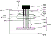
参照图3和图4A-4C,方法300从操作302开始,其中电介质层404形成在第一衬底402正面403上。如本文所用,术语结构的“正面”是指组件所形成的结构的那一侧。相反,如本文所用,术语“背面”是指与正面相对的结构的那一侧。为了便于说明,第一衬底402上、下颠倒地示出,使得第一衬底402的背面401在正面403上方。Referring to FIGS. 3 and 4A-4C ,
第一衬底402的材料可以是硅、锗、III-V半导体、碳化硅或硅覆绝缘衬底,或其组合。在一些实施例中,第一衬底402可包括硅(例如,单晶硅、多晶硅)、硅锗(SiGe)、砷化镓(GaAs)、锗(Ge)、绝缘体上硅(SOI)、绝缘体上锗(GOI),或其任何合适的组合。在一些实施例中,第一衬底402是硅晶圆。第一衬底402可包括一个或多个接触区域412,其中可形成多个接触。电介质层404形成在接触区域412中。在一些实施例中,电介质层404的材料可包括氧化物、氮化物或其组合。形成电介质层404的操作302包括但不限于光刻、蚀刻、沉积、填充、抛光或其组合。在一些实施例中,形成电介质层404的制造方法包括通过光刻和蚀刻工艺在第一衬底402的正面403的接触区域412中形成浅沟槽,用电介质材料沉积和填充浅沟槽,以及可选地通过抛光平坦化电介质层。在一些实施例中,电介质层404的背面405位于第一衬底402的正面403和背面401之间,以及电介质层404的正面407与第一衬底402的正面403处于相同的高度,如图4A所示。在一些实施例中,电介质层404的背面405位于第一衬底402的正面403和背面401之间,以及电介质层404的正面407高于第一衬底402的正面403,如图4B所示。在一些实施例中,形成电介质层404的制造方法包括在第一衬底402的正面403处沉积电介质层,以及可选地通过抛光平坦化所述电介质层。在一些实施例中,电介质层404的背面405与第一衬底402的正面403处于相同的高度,以及电介质层404的正面407高于第一衬底402的正面403,如图4C所示。在一些实施例中,电介质层404的厚度约介于200埃


形成电介质层404的示例性制造方法如图4A和4B所示,公开如下。首先,在第一衬底402(例如,硅晶圆)的正面403上形成图案化的硬屏蔽层,然后继续对第一衬底402进行蚀刻以形成浅沟槽。硬屏蔽层可包括通过化学气相沉积工艺形成的氮化硅层、通过高密度电浆化学气相沉积(HDPCVD)工艺形成的氧化硅层或其组合。可以使用本领域技术人员所知的任何公知技术蚀刻硬屏蔽层和第一衬底402以形成沟槽。其次,使用HDPCVD或本领域技术人员所知的任何公知技术在浅沟槽中和硬屏蔽层上填充电介质层。电介质层404的材料可包括但不限于氧化物、氮化物、氮氧化物,或以上组合等。在一些实施例中,电介质层404的材料可包括氧化硅、氮化硅、氮氧化硅或其组合。第三,通过化学机械抛光(CMP)方法或本领域技术人员所知的任何公知技术完全去除硬屏蔽层上的电介质层,以完全暴露硬屏蔽层的表面。第四,在400-800℃的环境温度下进行快速热氧化方法。在一些实施方案中,环境温度为500-700℃。在一些实施方案中,在快速热氧化工艺中,环境温度在60-140秒内线性加热至400-800℃。在一些实施例中,环境温度可以是例如450℃、480℃、550℃、600℃、660℃、640℃和750℃。线性加热时间可以是70秒、75秒、80秒、95秒、103秒、115秒、125秒、130秒。在一些实施方案中,快速热氧化方法可包括将含氧气体引入沟槽所处环境的操作。含氧气体可包括氧气(O2)、臭氧(O3)或具有氧化能力的任何其它气体。虽然不受任何特定理论或机制的束缚,但据信该操作可消除由先前制造工艺引起的对沟槽拐角处的原子结构的损害,并在后续流程中防止对沟槽拐角处的原子结构的进一步损坏。在快速热氧化工艺中,沟槽中的电介质层处于高温氧环境中,氧分子在高温环境中的浓度和分子活性很高。原始分子结构在沟槽的拐角处相对松散,因此在CMP工艺期间产生的游离硅离子可以在该过程中被完全氧化。并且沟槽中电介质层中新氧化的氧化物和原始氧化物分子可以在高温下形成稳定的分子键。沟槽中电介质层拐角处的松散氧化物结构变得坚固和致密,因此修复了由先前制造工艺引起的对沟槽拐角处原子结构的损坏。该高温氧化过程可称为高温淬火。最后,通过湿式蚀刻或本领域技术人员所知的任何公知技术去除硬屏蔽层。化学蚀刻剂的选择根据硬屏蔽层的材料而变化,以及是本领域技术人员已知的技术。Exemplary fabrication methods for forming
参照图3和图5,方法300进行到操作304,其中半导体结构520形成在第一衬底402的正面403上。在一些实施例中,位于第一衬底402的正面403处的半导体结构520可包括电介质层上的第一导电层510和第一导电接触506。第一导电接触510的第一端连接到第一导电层510,以及第一导电接触510的第二端延伸穿过电介质层的正面。在一些实施例中,半导体结构520是存储阵列结构,包括半导体组件层508、形成在半导体组件层508中并与接触区域412对准的第一导电接触506(例如,贯穿阵列接触(TAC)或接触通孔)、形成在接触区域412上和第一衬底402的正面403和半导体组件层508之间的电介质层404,以及在半导体组件层508的正面处的第一导电层510。形成半导体结构520包括但不限于光刻、蚀刻、沉积、填充、抛光或其组合。如本文所用,术语结构的“正面”是指形成组件的结构的那一面。相反,如本文所用,术语“背面”是指与正面相对的结构的那一面。为了便于说明,半导体结构520在图5-10中颠倒示出,使得半导体结构520的背面位于正面上方。然而,应当理解,在实际情形中,可以翻转半导体结构520,使得第一衬底402的背面401在制造工艺期间变为半导体结构520的底表面。Referring to FIGS. 3 and 5 , the
在一些实施例中,半导体组件层508可包括存储堆叠。在一些实施例中,通过重复堆叠多个存储单元来形成存储堆叠。在一些实施例中,半导体组件层508的厚度在约1μm和50μm之间。在一些实施例中,半导体组件层508的厚度在约5μm和50μm之间。在一些实施例中,半导体组件层508的厚度大于5μm。在一些实施例中,存储阵列堆叠通过多种制造方法形成,包括但不限于电介质层的薄膜沉积、沟道孔和狭缝的蚀刻、沟道孔中的存储薄膜的薄膜沉积,以与栅极和字符线置换。在一些实施例中,存储阵列堆叠可以形成(例如,设置)在第一衬底402的正面403,以及可以包括交替的导体/电介质堆叠和延伸通过交替的导体/电介质堆叠的NAND串的阵列。交替的导体/电介质堆叠可包括交替的导体层(例如,金属层或多晶硅层)和电介质层(例如,氧化硅层或氮化硅层)。每个NAND串可以包括多个垂直堆叠的存储单元,每个存储单元由围绕NAND串的交替导体/电介质堆叠的相应导体层(用作控制栅极)控制。交替导体/电介质堆叠中的导体层可以在存储阵列区域外部的横向方向上延伸,从而形成半导体结构520的字符线(例如,存储阵列结构)。每个NAND串还可以在末端(例如,在半导体结构520的正面)包括漏极。每个NAND串的漏极可以电连接到半导体结构520的多个位线中的相应一个。在一些实施例中,每个NAND串还包括多个选择栅极(例如,源极选择栅极和漏极选择栅极)。由于相关领域的技术人员能够理解该段中描述的一些结构,故这些结构未在图5中示出。In some embodiments, the
半导体结构520可包括一个或多个第一导电接触506(TAC或接触通孔),每个第一导电接触506垂直延伸穿过半导体结构520的至少一部分。在一些实施例中,第一导电接触506可垂直延伸穿过整个半导体结构520,即,在半导体结构520的正面和背面的两个标称平行表面之间。例如,第一导电接触506可以穿过整个半导体组件层508和整个第一衬底402。在一些实施例中,第一导电接触506可以垂直延伸通过半导体结构520的一部分。在一些实施例中,第一导电接触506可以穿过整个半导体组件层508和部分电介质层404。在一些实施例中,第一导电接触506可以穿过整个半导体组件层508和整个电介质层404,使得第一导电接触506到达电介质层404的背面405。在一些实施例中,第一导电接触506可以穿过整个半导体组件层508和第一衬底402的一部分。在一些实施例中,第一导电接触506可以穿过半导体组件层508的一部分而不到达第一衬底402。在一些实施例中,第一导电接触506在一端与电介质层404接触,并在另一端与第一导电层510接触。The
每个接触506可包括填充有导体材料的垂直开口,所述导体材料包括但不限于钨(W)、钴(Co)、铜(Cu)、铝(Al)、掺杂硅、硅化物或其组合。Each
在一些实施例中,接触的直径约介于0.3μm至5μm之间。在一些实施例中,接触的直径约介于0.3μm至0.5μm之间。在一些实施例中,接触的直径约介于1μm至5μm之间。In some embodiments, the diameter of the contacts is between about 0.3 μm and 5 μm. In some embodiments, the diameter of the contacts is between about 0.3 μm and 0.5 μm. In some embodiments, the diameter of the contacts is between about 1 μm and 5 μm.
第一导电接触506可以位于存储阵列区域中及/或存储阵列区域外部,例如,在半导体结构520的阶梯区域中。第一导电接触506可以与字符线接触、位线接触及选择栅极接触形成电性连结。字符线接触可以在阶梯区域中并且电连接到字符线,使得每个字符线接触可以单独地寻址相应的字符线。位线接触可以通过位线电连接到NAND串,使得每个位线接触可以单独地寻址相应的NAND串。选择栅极接触可以电连接到选择栅极。由于该段中描述的一些结构是相关领域的技术人员能理解的,因此这些结构未在图5中示出。The first
半导体结构520可以包括在半导体组件层508的正面的第一导电层510。第一导电层510可以提供与存储阵列结构及/或周边组件结构的连接。可以基于存储阵列组件的内部结构及/或周边组件结构的布局来图案化第一导电层510,从而可以形成合适的互连结构。第一导电层510可包括但不限于W、Co、Cu、Al、金属硅化物或任何其它合适的材料。The
参照图3和图6,方法300进行到操作306和308,其中第二衬底616连接到半导体结构520,接着是第一衬底402的背面的减薄工艺,以形成衬底602,和第一钝化层614的沉积。如图6所示,衬底616可以通过键合工艺连接到半导体结构520的正面。在一些实施例中,键合工艺可包括黏合剂键合、阳极键合、直接晶圆键合、共晶键合、混合金属/电介质键合或其组合。黏合剂键合,也称为胶合或胶黏键合,是一种晶圆键合技术,其施加中间层以连接不同材料的衬底。阳极键合是将玻璃密封到硅或金属而不引入中间层的晶圆键合工艺,通常用于通过电场将玻璃密封到电子和微流道的硅晶圆。直接键合(也称为熔融键合)是晶圆键合工艺,没有任何另外的中间层。直接键合工艺基于满足特定要求的两个材料表面之间的化学键。直接键合工艺可包括晶圆预处理、室温下预键合和在升温下进行退火。共晶键合,也称为共晶焊接,是具有可以产生共晶系统的中间金属层的晶圆键合技术。混合键合,也称为“金属/电介质混合键合”,可以是直接键合技术(例如,在不使用中间层的情况下在表面之间形成键合,诸如焊料或黏合剂),其同时获得金属-金属键合和电介质-电介质键合。3 and 6, the
衬底616的材料可以是硅、锗、III-V半导体、碳化硅或硅覆绝缘衬底,或其组合。在一些实施例中,第二衬底616可包括硅(例如,单晶硅、多晶硅)、硅锗(SiGe)、砷化镓(GaAs)、锗(Ge)、绝缘体上硅(SOI)、绝缘体上锗(GOI),或其任何合适的组合。在一些实施例中,第二衬底616是硅晶圆。The material of the
在一些实施例中,第一钝化层614的厚度约介于


然后通过包括但不限于机械研磨(例如,抛光)、化学机械平坦化、湿式蚀刻和大气下游电浆干化学蚀刻等技术从背面减薄第一衬底602。在一些实施例中,衬底602的厚度约介于0.5μm和20μm之间。在一些实施例中,衬底602的厚度约介于0.5μm和5μm之间。在一些实施例中,衬底602的厚度约介于5μm和20μm之间。The
在一些实施例中,在执行减薄工艺之后,在第一衬底402(衬底602)的背面沉积第一钝化层614。第一钝化层614的材料可包括氧化物、氮化物、氮氧化物或其组合。在一些实施例中,第一钝化层614包括氧化硅、氮化硅、氮氧化硅或其组合。第一钝化层614可以通过一种或多种薄膜沉积工艺(诸如原子层沉积(ALD)、化学气相沉积(CVD)、物理气相沉积(PVD)或其组合)形成。In some embodiments, after performing the thinning process, a
参照图3和图7,方法300进行到操作310,其中在第一钝化层614和衬底602中形成多个穿孔718。如图7所示,穿孔718延伸穿过衬底602的背面401和电介质层404的一部分。在一些实施例中,穿孔718可与第一导电接触506对准,以及第一导电接触506从穿孔718暴露。在一些实施例中,用于形成穿孔718的制造方法包括形成多个孔垂直延伸穿过第一钝化层614和衬底602,所述多个孔使用包括但不限于光刻、蚀刻、沉积绝缘层或其组合等技术形成。然后,在第二导电接触的侧壁和第一衬底之间沉积绝缘层722,以形成绝缘衬垫。绝缘层722的材料可包括氧化物、氮化物、氮氧化物或其组合。在一些实施例中,绝缘层722包括氧化硅、氮化硅、氮氧化硅或其组合。绝缘层722可以通过一种或多种薄膜沉积方法(诸如ALD、CVD、PVD或其组合)形成。Referring to FIGS. 3 and 7 , the
参照图3和图8,方法300进行到操作312,其中通过将导电材料设置到多个穿孔718中而在第一衬底602的背面形成第二导电接触824。如图8所示,利用ALD、CVD、PVD,任何其它合适的方法或其组合,使导电材料填充穿孔718。用于填充穿孔718的导体材料可包括但不限于W、Co、Cu、Al、Sn、多晶硅、硅化物或其组合。在一些实施例中,其它导体材料也用于填充开口以用作阻挡层、黏附层及/或种子层。在一些实施例中,填充在穿孔718中的导电材料与第一导电接触506电连接。在一些实施例中,穿孔718的直径约介于0.3μm和5μm之间。在一些实施例中,穿孔718的直径约介于0.3μm和1μm之间。在一些实施例中,穿孔718的直径约介于1μm和5μm之间。Referring to FIGS. 3 and 8 ,
参照图3和图9,方法300进行到操作314,其中导电布线层926形成在第一衬底的背面。如图9所示,在第一衬底602的背面沉积导电层并通过光刻和蚀刻图案化以形成导电布线层926。导电布线层926可以与第二导电接触824形成电连接。在一些实施例中,导电布线层926可以与第一导电接触506、第一导电层510及/或第二衬底616形成电连接。可以基于存储阵列组件及/或周边组件结构的内部结构的布局来图案化导电布线层926,从而可以形成合适的互连结构。导电布线层926可包括但不限于W、Co、Cu、Al、Ag、Sn、金属硅化物或任何其它合适的材料。在一些实施例中,导电布线层926位于半导体结构520的背面处的一个或多个BEOL互连层(未示出)之中或之上。3 and 9, the
在一些实施例中,为了减小由导电布线层926引起的半导体结构520的应力,导电布线层926和半导体组件层508之间在垂直方向上的距离为至少约3μm。例如,半导体结构520的第一衬底402和导电布线层926下面的BEOL互连层的总和厚度可以是至少约3μm。在一些实施例中,导电布线层926和半导体组件层508之间的垂直距离约介于3μm和10μm之间(例如,约3μm、约4μm、约5μm、约6μm、约7μm、约8μm、约9μm、约10μm,在由这些值中的任何值限定的下端上限定的任何范围内,或在由这些值中的任何两个限定的任何范围内)。在一些实施例中,导电布线层926可以完全与半导体结构520重迭。在一些实施例中,导电布线层926可以部分地与半导体结构520重迭。In some embodiments, to reduce stress on
参照图3和图10,方法300进行到操作316,其中第二钝化层1028形成在半导体结构520的背面。如图10所示,在半导体结构520的背面的导电布线层926和第一钝化层614上方沉积第二钝化层1028。第二钝化层1028的材料可包括氧化物、氮化物、氮氧化物或其组合。在一些实施例中,第二钝化层1028包括氧化硅、氮化硅、氮氧化硅或其组合。第二钝化层1028可以通过一种或多种薄膜沉积方法(诸如ALD、CVD、PVD或其组合)形成。可以基于存储阵列组件的内部结构及/或周边组件结构的布局来图案化第二钝化层1028,从而可以形成合适的互连结构。Referring to FIGS. 3 and 10 , the
在一些实施例中,3D存储组件还可以包括衬底616上的周边组件结构(未示出),其面对面地定位,其前侧面向存储阵列结构。周边组件可以包括用于促进3D存储组件操作的任何合适的数字、模拟及/或混合信号周边电路。例如,周边组件可以包括页面缓冲器、译码器(例如,行译码器和列译码器)、驱动器、电荷泵、电流或电压参考或者电路中的任何主动或被动组件中的一个或多个(例如,晶体管、二极管、电阻器或电容器)。在一些实施例中,使用CMOS技术形成周边组件。In some embodiments, the 3D memory assembly may also include perimeter assembly structures (not shown) on
在一些实施例中,提供了一种半导体组件的3D集成布线结构,其中3D集成布线结构通过上述任一实施例中描述的方法制成。在一些实施例中,半导体组件是3D存储组件。在一些实施例中,3D集成布线结构包括具有多个接触的存储组件层,以及第一导电层。在一些实施例中,多个接触在一端连接到电介质层并且在另一端连接到第一导电层。In some embodiments, a 3D integrated wiring structure of a semiconductor component is provided, wherein the 3D integrated wiring structure is fabricated by the method described in any of the above embodiments. In some embodiments, the semiconductor components are 3D memory components. In some embodiments, a 3D integrated wiring structure includes a memory component layer having a plurality of contacts, and a first conductive layer. In some embodiments, the plurality of contacts are connected to the dielectric layer at one end and to the first conductive layer at the other end.
根据本公开内容的各种实施例提供了用于形成3D集成布线结构的方法和具有互连结构的半导体组件。所公开的用于形成3D集成布线结构的方法可以包括在第一衬底中形成电介质层;形成在第一衬底的正面上具有第一导电接触的半导体结构;在所述第一衬底的背面形成第二导电接触,其中所述第二导电接触延伸穿过所述电介质层的背面并连接到所述第一导电接触的第二端。因此,所公开的用于形成3D集成布线结构的方法可以提供互连结构并且能够通过厚半导体组件层布线。Various embodiments in accordance with the present disclosure provide methods for forming 3D integrated wiring structures and semiconductor assemblies having interconnect structures. The disclosed method for forming a 3D integrated wiring structure may include forming a dielectric layer in a first substrate; forming a semiconductor structure having a first conductive contact on a front side of the first substrate; The backside forms a second conductive contact, wherein the second conductive contact extends through the backside of the dielectric layer and connects to the second end of the first conductive contact. Thus, the disclosed methods for forming 3D integrated wiring structures can provide interconnect structures and enable wiring through thick semiconductor component layers.
在一些实施例中,公开了一种用于形成3D集成布线结构的方法。在第一衬底中形成电介质层。在第一衬底的正面上形成半导体结构。半导体结构包括电介质层上方的第一导电层和第一导电接触。第一导电接触的第一端连接到第一导电层,第一导电接触的第二端延伸穿过电介质层的正面。第二导电接触形成在第一衬底的背面。第二导电接触延伸穿过电介质层的背面并连接到第一导电接触的第二端。In some embodiments, a method for forming a 3D integrated wiring structure is disclosed. A dielectric layer is formed in the first substrate. A semiconductor structure is formed on the front side of the first substrate. The semiconductor structure includes a first conductive layer and a first conductive contact over the dielectric layer. The first end of the first conductive contact is connected to the first conductive layer, and the second end of the first conductive contact extends through the front surface of the dielectric layer. A second conductive contact is formed on the backside of the first substrate. The second conductive contact extends through the backside of the dielectric layer and connects to the second end of the first conductive contact.
在一些实施例中,公开了一种具有3D集成布线结构的结构。3D集成布线结构可包括:第一衬底,具有正面和背面;第一衬底中的电介质层;半导体结构,位于第一衬底的正面上方,具有第一导电接触;以及在第一衬底的背面上的第二导电接触,以及第二导电接触延伸穿过电介质层的背面并连接到第一导电接触的第二端。在一些实施例中,半导体结构包括电介质层上方的第一导电层和第一导电接触。在一些实施例中,第一导电接触的第一端连接到第一导电层,以及第一导电接触的第二端延伸穿过电介质层的正面。在一些实施例中,半导体结构是3D存储结构。In some embodiments, a structure with a 3D integrated wiring structure is disclosed. The 3D integrated wiring structure may include: a first substrate having a front side and a back side; a dielectric layer in the first substrate; a semiconductor structure over the front side of the first substrate having a first conductive contact; A second conductive contact on the backside of the , and the second conductive contact extends through the backside of the dielectric layer and connects to the second end of the first conductive contact. In some embodiments, the semiconductor structure includes a first conductive layer and a first conductive contact over a dielectric layer. In some embodiments, the first end of the first conductive contact is connected to the first conductive layer, and the second end of the first conductive contact extends through the front side of the dielectric layer. In some embodiments, the semiconductor structure is a 3D memory structure.
对特定实施例的上述说明将完全地展现本公开内容的一般性质,使得他人能够通过运用本领域技术范围内的知识容易地对这样的特定实施例进行修改及/或调整以用于各种应用,而不需要过度实验,不脱离本公开内容的一般概念。因此,基于本文呈现的教导和指导,这样的调整和修改旨在处于所公开的实施例的等效物的含义和范围内。应当理解,本文中的措辞或术语是出于说明的目的,而不是为了进行限制,从而本说明书的术语或措辞将由技术人员按照所述教导和指导进行解释。The foregoing descriptions of specific embodiments will fully demonstrate the general nature of the disclosure, enabling others to readily modify and/or adapt such specific embodiments for various applications by employing knowledge within the skill in the art , without undue experimentation, without departing from the general concept of the present disclosure. Therefore, such adaptations and modifications are intended to be within the meaning and range of equivalents of the disclosed embodiments, based on the teaching and guidance presented herein. It is to be understood that the phraseology or terminology herein is for the purpose of description and not limitation so that the term or phraseology of this specification will be interpreted by a skilled artisan in accordance with the teaching and guidance.
上文已经借助于功能构建块描述了本公开内容的实施例,功能构建块例示了指定功能及其关系的实施方式。在本文中出于方便描述的目的任意地定义了这些功能构建块的边界。可以定义替代的边界,只要适当执行指定的功能及其关系即可。Embodiments of the present disclosure have been described above with the aid of functional building blocks that illustrate implementations of specified functions and relationships thereof. The boundaries of these functional building blocks are arbitrarily defined herein for convenience of description. Alternate boundaries may be defined so long as the specified functions and relationships thereof are appropriately performed.
发明内容和摘要部分可以阐述发明人所设想的本公开内容的一个或多个示例性实施例,但未必是所有示例性实施例,以及因此,并非旨在通过任何方式限制本公开内容和所附权利要求。The Summary and Abstract sections may set forth one or more, but not necessarily all, exemplary embodiments of the present disclosure contemplated by the inventors, and, accordingly, are not intended to limit the present disclosure and the accompanying drawings in any way. Rights request.
本公开内容的广度和范围不应受任何上述示例性实施例的限制,以及应当仅根据以下权利要求书及其等效物来进行限定。The breadth and scope of the present disclosure should not be limited by any of the above-described exemplary embodiments, and should be limited only in accordance with the following claims and their equivalents.
Claims (20)
Priority Applications (1)
| Application Number | Priority Date | Filing Date | Title |
|---|---|---|---|
| CN202010428940.6A CN111446207B (en) | 2017-08-31 | 2018-06-08 | Method of forming three-dimensional integrated wiring structure and semiconductor structure thereof |
Applications Claiming Priority (3)
| Application Number | Priority Date | Filing Date | Title |
|---|---|---|---|
| CN201710774763.5A CN107644837B (en) | 2017-08-31 | 2017-08-31 | Wafer three-dimensional integration lead technique and its structure for three-dimensional storage |
| CN2017107747635 | 2017-08-31 | ||
| PCT/CN2018/090457 WO2019041956A1 (en) | 2017-08-31 | 2018-06-08 | Method for forming three-dimensional integrated wiring structure and semiconductor structure thereof |
Related Child Applications (1)
| Application Number | Title | Priority Date | Filing Date |
|---|---|---|---|
| CN202010428940.6A Division CN111446207B (en) | 2017-08-31 | 2018-06-08 | Method of forming three-dimensional integrated wiring structure and semiconductor structure thereof |
Publications (2)
| Publication Number | Publication Date |
|---|---|
| CN110114867A CN110114867A (en) | 2019-08-09 |
| CN110114867B true CN110114867B (en) | 2020-06-26 |
Family
ID=61110148
Family Applications (3)
| Application Number | Title | Priority Date | Filing Date |
|---|---|---|---|
| CN201710774763.5A Active CN107644837B (en) | 2017-08-31 | 2017-08-31 | Wafer three-dimensional integration lead technique and its structure for three-dimensional storage |
| CN202010428940.6A Active CN111446207B (en) | 2017-08-31 | 2018-06-08 | Method of forming three-dimensional integrated wiring structure and semiconductor structure thereof |
| CN201880005423.9A Active CN110114867B (en) | 2017-08-31 | 2018-06-08 | Method of forming three-dimensional integrated wiring structure and semiconductor structure thereof |
Family Applications Before (2)
| Application Number | Title | Priority Date | Filing Date |
|---|---|---|---|
| CN201710774763.5A Active CN107644837B (en) | 2017-08-31 | 2017-08-31 | Wafer three-dimensional integration lead technique and its structure for three-dimensional storage |
| CN202010428940.6A Active CN111446207B (en) | 2017-08-31 | 2018-06-08 | Method of forming three-dimensional integrated wiring structure and semiconductor structure thereof |
Country Status (3)
| Country | Link |
|---|---|
| CN (3) | CN107644837B (en) |
| TW (1) | TWI707412B (en) |
| WO (1) | WO2019041956A1 (en) |
Families Citing this family (13)
| Publication number | Priority date | Publication date | Assignee | Title |
|---|---|---|---|---|
| US10651087B2 (en) | 2017-08-31 | 2020-05-12 | Yangtze Memory Technologies Co., Ltd. | Method for forming three-dimensional integrated wiring structure and semiconductor structure thereof |
| WO2019042250A1 (en) * | 2017-08-31 | 2019-03-07 | 长江存储科技有限责任公司 | Memory structure and forming method thereof |
| CN107644837B (en) * | 2017-08-31 | 2019-01-01 | 长江存储科技有限责任公司 | Wafer three-dimensional integration lead technique and its structure for three-dimensional storage |
| US10607887B2 (en) | 2017-08-31 | 2020-03-31 | Yangtze Memory Technologies Co., Ltd. | Method for forming three-dimensional integrated wiring structure and semiconductor structure thereof |
| CN108511473B (en) * | 2018-03-12 | 2021-04-20 | 佛山市海森特集成电路有限公司 | Interconnection process for metal layers between wafers |
| CN108511350B (en) * | 2018-05-14 | 2020-09-01 | 南京溧水高新创业投资管理有限公司 | Packaging method of power device and power device |
| CN109196643B (en) | 2018-06-12 | 2019-11-05 | 长江存储科技有限责任公司 | Memory device and forming method thereof |
| CN109037225B (en) * | 2018-09-19 | 2023-09-12 | 长江存储科技有限责任公司 | memory structure |
| KR102554692B1 (en) * | 2019-02-18 | 2023-07-12 | 양쯔 메모리 테크놀로지스 씨오., 엘티디. | Integrated structure and formation method |
| DE102019211468A1 (en) | 2019-07-31 | 2021-02-04 | Fraunhofer-Gesellschaft zur Förderung der angewandten Forschung e.V. | VERTICAL CONNECTING SEMI-CONDUCTOR STRUCTURE AND METHOD OF MAKING THE SAME |
| DE102019211465A1 (en) * | 2019-07-31 | 2021-02-04 | Fraunhofer-Gesellschaft zur Förderung der angewandten Forschung e.V. | SEMICONDUCTOR COMPONENT STRUCTURE WITH CONNECTING SEMICONDUCTORS AND PROCESS FOR PRODUCING THE SAME |
| CN111223871B (en) * | 2020-01-14 | 2023-07-04 | 长江存储科技有限责任公司 | Preparation method of memory device and memory device |
| CN111326511A (en) * | 2020-03-09 | 2020-06-23 | 长江存储科技有限责任公司 | Memory device and method of manufacturing the same |
Citations (3)
| Publication number | Priority date | Publication date | Assignee | Title |
|---|---|---|---|---|
| CN104428887A (en) * | 2012-07-09 | 2015-03-18 | 高通股份有限公司 | Integrating through substrate vias from wafer backside layers of integrated circuits |
| CN104810396A (en) * | 2014-01-23 | 2015-07-29 | 中芯国际集成电路制造(上海)有限公司 | Semiconductor device and manufacture method thereof |
| CN106992162A (en) * | 2016-01-19 | 2017-07-28 | 三星电子株式会社 | Multiple stacking device with TSV structure |
Family Cites Families (7)
| Publication number | Priority date | Publication date | Assignee | Title |
|---|---|---|---|---|
| US7396732B2 (en) * | 2004-12-17 | 2008-07-08 | Interuniversitair Microelektronica Centrum Vzw (Imec) | Formation of deep trench airgaps and related applications |
| JP5302522B2 (en) * | 2007-07-02 | 2013-10-02 | スパンション エルエルシー | Semiconductor device and manufacturing method thereof |
| US8791525B2 (en) * | 2008-02-25 | 2014-07-29 | International Rectifier Corporation | Power semiconductor device including a double metal contact |
| WO2009115449A1 (en) * | 2008-03-19 | 2009-09-24 | Interuniversitair Microelektronica Centrum Vzw (Imec) | Method for fabricating through-substrate vias |
| US8791575B2 (en) * | 2010-07-23 | 2014-07-29 | Tessera, Inc. | Microelectronic elements having metallic pads overlying vias |
| KR20140028969A (en) * | 2012-08-31 | 2014-03-10 | 에스케이하이닉스 주식회사 | Semiconductor device and manufacturing method of the same |
| CN107644837B (en) * | 2017-08-31 | 2019-01-01 | 长江存储科技有限责任公司 | Wafer three-dimensional integration lead technique and its structure for three-dimensional storage |
-
2017
- 2017-08-31 CN CN201710774763.5A patent/CN107644837B/en active Active
-
2018
- 2018-06-08 CN CN202010428940.6A patent/CN111446207B/en active Active
- 2018-06-08 CN CN201880005423.9A patent/CN110114867B/en active Active
- 2018-06-08 WO PCT/CN2018/090457 patent/WO2019041956A1/en active Application Filing
- 2018-06-29 TW TW107122421A patent/TWI707412B/en active
Patent Citations (3)
| Publication number | Priority date | Publication date | Assignee | Title |
|---|---|---|---|---|
| CN104428887A (en) * | 2012-07-09 | 2015-03-18 | 高通股份有限公司 | Integrating through substrate vias from wafer backside layers of integrated circuits |
| CN104810396A (en) * | 2014-01-23 | 2015-07-29 | 中芯国际集成电路制造(上海)有限公司 | Semiconductor device and manufacture method thereof |
| CN106992162A (en) * | 2016-01-19 | 2017-07-28 | 三星电子株式会社 | Multiple stacking device with TSV structure |
Also Published As
| Publication number | Publication date |
|---|---|
| CN110114867A (en) | 2019-08-09 |
| TW201913841A (en) | 2019-04-01 |
| CN107644837B (en) | 2019-01-01 |
| WO2019041956A1 (en) | 2019-03-07 |
| CN111446207A (en) | 2020-07-24 |
| TWI707412B (en) | 2020-10-11 |
| CN107644837A (en) | 2018-01-30 |
| CN111446207B (en) | 2021-05-07 |
Similar Documents
| Publication | Publication Date | Title |
|---|---|---|
| CN110114867B (en) | Method of forming three-dimensional integrated wiring structure and semiconductor structure thereof | |
| US11527547B2 (en) | Hybrid bonding contact structure of three-dimensional memory device | |
| CN112951838B (en) | 3D memory device | |
| CN109314116B (en) | The method for being used to form three-dimensional storage part | |
| CN110140213B (en) | Three-dimensional memory device and manufacturing method thereof | |
| CN111415941B (en) | Multi-layer stacked three-dimensional memory device | |
| TWI689079B (en) | Inter-stack plug in three-dimensional memory element and method of forming same | |
| CN110088889B (en) | Method for forming three-dimensional integrated wiring structure and semiconductor structure thereof | |
| US11056387B2 (en) | Method for forming three-dimensional integrated wiring structure and semiconductor structure thereof | |
| TW202234676A (en) | Semiconductor device and three-dimensional memory device | |
| US10796993B2 (en) | Method for forming three-dimensional integrated wiring structure and semiconductor structure thereof | |
| US11791265B2 (en) | Method for forming three-dimensional integrated wiring structure and semiconductor structure thereof | |
| US10607887B2 (en) | Method for forming three-dimensional integrated wiring structure and semiconductor structure thereof |
Legal Events
| Date | Code | Title | Description |
|---|---|---|---|
| PB01 | Publication | ||
| PB01 | Publication | ||
| SE01 | Entry into force of request for substantive examination | ||
| SE01 | Entry into force of request for substantive examination | ||
| GR01 | Patent grant | ||
| GR01 | Patent grant |