CN100336169C - Manufacturing method and structure of inductance element - Google Patents
Manufacturing method and structure of inductance element Download PDFInfo
- Publication number
- CN100336169C CN100336169C CNB2004100050416A CN200410005041A CN100336169C CN 100336169 C CN100336169 C CN 100336169C CN B2004100050416 A CNB2004100050416 A CN B2004100050416A CN 200410005041 A CN200410005041 A CN 200410005041A CN 100336169 C CN100336169 C CN 100336169C
- Authority
- CN
- China
- Prior art keywords
- inductive graph
- metal
- inductance element
- inductive
- graph
- Prior art date
- Legal status (The legal status is an assumption and is not a legal conclusion. Google has not performed a legal analysis and makes no representation as to the accuracy of the status listed.)
- Expired - Lifetime
Links
- 238000004519 manufacturing process Methods 0.000 title claims abstract description 34
- 238000000034 method Methods 0.000 claims abstract description 75
- 239000000758 substrate Substances 0.000 claims abstract description 45
- 229910052751 metal Inorganic materials 0.000 claims description 199
- 239000002184 metal Substances 0.000 claims description 199
- 230000001939 inductive effect Effects 0.000 claims description 69
- 239000000463 material Substances 0.000 claims description 19
- 229910052782 aluminium Inorganic materials 0.000 claims description 5
- XAGFODPZIPBFFR-UHFFFAOYSA-N aluminium Chemical compound [Al] XAGFODPZIPBFFR-UHFFFAOYSA-N 0.000 claims description 5
- 230000015572 biosynthetic process Effects 0.000 claims description 4
- 230000006698 induction Effects 0.000 claims 9
- 239000007787 solid Substances 0.000 claims 6
- 239000004411 aluminium Substances 0.000 claims 1
- 230000001965 increasing effect Effects 0.000 abstract description 15
- 239000010410 layer Substances 0.000 description 175
- 238000005530 etching Methods 0.000 description 9
- 238000000151 deposition Methods 0.000 description 7
- XUIMIQQOPSSXEZ-UHFFFAOYSA-N Silicon Chemical compound [Si] XUIMIQQOPSSXEZ-UHFFFAOYSA-N 0.000 description 5
- 230000008021 deposition Effects 0.000 description 5
- 229910052710 silicon Inorganic materials 0.000 description 5
- 239000010703 silicon Substances 0.000 description 5
- RYGMFSIKBFXOCR-UHFFFAOYSA-N Copper Chemical compound [Cu] RYGMFSIKBFXOCR-UHFFFAOYSA-N 0.000 description 4
- 229910052802 copper Inorganic materials 0.000 description 4
- 239000010949 copper Substances 0.000 description 4
- 239000007769 metal material Substances 0.000 description 4
- 238000005498 polishing Methods 0.000 description 4
- 239000000126 substance Substances 0.000 description 4
- 238000005229 chemical vapour deposition Methods 0.000 description 3
- 239000004065 semiconductor Substances 0.000 description 3
- WFKWXMTUELFFGS-UHFFFAOYSA-N tungsten Chemical compound [W] WFKWXMTUELFFGS-UHFFFAOYSA-N 0.000 description 3
- 229910052721 tungsten Inorganic materials 0.000 description 3
- 239000010937 tungsten Substances 0.000 description 3
- 229910052581 Si3N4 Inorganic materials 0.000 description 2
- VYPSYNLAJGMNEJ-UHFFFAOYSA-N Silicium dioxide Chemical compound O=[Si]=O VYPSYNLAJGMNEJ-UHFFFAOYSA-N 0.000 description 2
- 238000010586 diagram Methods 0.000 description 2
- 239000003989 dielectric material Substances 0.000 description 2
- 238000005240 physical vapour deposition Methods 0.000 description 2
- HQVNEWCFYHHQES-UHFFFAOYSA-N silicon nitride Chemical compound N12[Si]34N5[Si]62N3[Si]51N64 HQVNEWCFYHHQES-UHFFFAOYSA-N 0.000 description 2
- 229910052814 silicon oxide Inorganic materials 0.000 description 2
- 238000004891 communication Methods 0.000 description 1
- 239000004020 conductor Substances 0.000 description 1
- 238000005137 deposition process Methods 0.000 description 1
- 230000009977 dual effect Effects 0.000 description 1
- 230000000694 effects Effects 0.000 description 1
- 238000005516 engineering process Methods 0.000 description 1
- 238000004021 metal welding Methods 0.000 description 1
- 238000012986 modification Methods 0.000 description 1
- 230000004048 modification Effects 0.000 description 1
- 239000011241 protective layer Substances 0.000 description 1
- 238000004544 sputter deposition Methods 0.000 description 1
Images


Landscapes
- Semiconductor Integrated Circuits (AREA)
- Coils Or Transformers For Communication (AREA)
Abstract
Description
技术领域technical field
本发明是有关于一种半导体元件的制造方法与结构,且特别是有关于一种电感元件的制造方法与结构。The present invention relates to a manufacturing method and structure of a semiconductor element, and in particular to a manufacturing method and structure of an inductance element.
背景技术Background technique
在集成电路中,电感元件是一种重要的元件,这些电感元件样式一般是为圆形或方形的螺旋状金属线圈,而且这些电感元件的应用范围可以说是相当地广泛。以高频的应用领域来说,其对于电感元件的品质要求较高,意即应用在该领域的电感元件其具有较高的Q值。例如在无线通讯的应用上,电感元件的Q值必须达到60左右。上述Q值的定义如下:In an integrated circuit, an inductance element is an important element, and the style of these inductance elements is generally a circular or square helical metal coil, and the application range of these inductance elements can be said to be quite wide. For the application field of high frequency, it has higher requirements on the quality of the inductance element, which means that the inductance element used in this field has a higher Q value. For example, in the application of wireless communication, the Q value of the inductance element must reach about 60. The definition of the above Q value is as follows:
Q=ω0L/R (1)Q= ω0 L/R (1)
其中ω0为电感元件的共振角频率(resonant angular frequency),R为电感元件的电阻,而L为金属线圈的电感元件值。Where ω 0 is the resonant angular frequency of the inductance element, R is the resistance of the inductance element, and L is the value of the inductance element of the metal coil.
由第(1)式可知,在L固定下,Q值会随着共振角频率的增加和/或电阻下降而提高,其中电阻又和电流密度的平方成正比,所以要提高Q值的方法之一为增加金属线圈的截面积来降低金属线圈电流密度,以此方式来降低金属线圈的电阻,达成提高Q值的目的。It can be seen from the formula (1) that when L is fixed, the Q value will increase with the increase of the resonance angular frequency and/or the decrease of the resistance, and the resistance is proportional to the square of the current density, so one of the methods to increase the Q value is One is to increase the cross-sectional area of the metal coil to reduce the current density of the metal coil, thereby reducing the resistance of the metal coil and achieving the purpose of increasing the Q value.
所以,在半导体工序中若要以增加金属导线截面积来制造高Q值电感元件,可以通过加粗金属导线宽度的方式来完成。但是若金属导线的宽度太大时,又会因为电荷倾向集中分布于金属导线的转角处,而使得金属导线所增加的截面积无法达成降低金属导线电流密度的效果,也就无法提高由金属导线所组成的电感元件的Q值。因此,一般以半导体工序所能制造出的电感元件,其Q值最多只能到10左右。Therefore, in the semiconductor process, if the cross-sectional area of the metal wire is to be increased to manufacture a high-Q inductance element, it can be done by increasing the width of the metal wire. However, if the width of the metal wire is too large, the charge tends to be concentrated and distributed at the corner of the metal wire, so that the increased cross-sectional area of the metal wire cannot achieve the effect of reducing the current density of the metal wire, and it is impossible to increase the current density of the metal wire. The Q value of the composed inductive element. Therefore, generally, the Q value of the inductance element that can be manufactured by the semiconductor process can only reach about 10 at most.
而且,大部分的电感元件都配置于晶片的保护层下方,所以电感元件很接近硅衬底(<10μm以下),因此,在使用高频元件的高频率之下,硅衬底会变成导体,并且消耗掉大量的能量,使得电感元件的品质降低。Moreover, most of the inductance components are arranged under the protective layer of the chip, so the inductance components are very close to the silicon substrate (less than 10 μm), therefore, the silicon substrate will become a conductor at high frequencies using high-frequency components , and consume a large amount of energy, which reduces the quality of the inductive element.
尚且,虽然公知技术提出通过金属内连线工序形成由金属导线/介层窗/金属导线构成的立体电感元件,然而,该电感元件同样具有过于接近硅衬底的问题,再者,其中的介层窗层受到工艺限制,并无法制作成与金属导线层具有相似的图形,而仅能形成多数的插塞以连接上下两层金属导线层,因而无法进一步提高电感元件的Q值。所以,如何解决上述问题,并且提高电感元件的品质与其Q值是目前工序所关心的问题。Moreover, although the known technology proposes to form a three-dimensional inductance element composed of metal wires/vias/metal wires through the metal interconnection process, however, the inductance element also has the problem of being too close to the silicon substrate. The layer window layer is limited by the process and cannot be made into a pattern similar to the metal wire layer, but only a large number of plugs can be formed to connect the upper and lower metal wire layers, so the Q value of the inductance element cannot be further improved. Therefore, how to solve the above-mentioned problems and improve the quality and Q value of the inductance element is a concern of the current process.
发明内容Contents of the invention
有鉴于此,本发明的目的就是在提供一种电感元件的制作方法,该方法能在不额外增加工序步骤情况下,降低电感元件的阻抗,并改善电感元件的Q值。In view of this, the object of the present invention is to provide a method for manufacturing an inductance element, which can reduce the impedance of the inductance element and improve the Q value of the inductance element without adding additional process steps.
本发明的另一目的是提供一种电感元件结构,该电感元件结构可以使电感元件结构较远离硅衬底,以降低硅衬底对电感元件所造成的导磁干扰,以提高晶片效能。Another object of the present invention is to provide an inductance element structure, which can make the inductance element structure far away from the silicon substrate, so as to reduce the magnetic interference caused by the silicon substrate to the inductance element, so as to improve the performance of the chip.
本发明的再一目的是提供一种电感元件结构,该电感元件是为多层结构且整个电感元件具有均一的厚度,而能够增加电感元件的Q值。Another object of the present invention is to provide an inductance element structure, the inductance element has a multi-layer structure and the entire inductance element has a uniform thickness, so that the Q value of the inductance element can be increased.
本发明提出一种电感元件的制造方法,该方法是架构于衬底上,该衬底上至少形成有第一介电层,该电感元件的制作方法是首先于第一介电层上同时形成图形化的第一金属层与第一电感图形。之后,形成图形化的第二介电层于第一介电层上,以覆盖第一金属层、第一电感图形与第一介电层,且此第二介电层具有数个第一开口与数个第二开口,其中第一开口暴露出第一金属层,且第二开口暴露出第一电感图形。然后,于第一开口与第二开口中填入金属,以同时于第一开口中形成第二金属层,且于第二开口中形成第二电感图形,其中第二金属层与第一金属层电连接,而第二电感图形与第一电感图形电连接。接着,于第二金属层上形成图形化的第三金属层,并且同时于第二电感图形上形成第三电感图形,其中第三金属层与第二金属层电连接,且第三电感图形与第二电感图形电连接,并且第一电感图形、第二电感图形与第三电感图形具有相似的图形。The present invention proposes a method for manufacturing an inductance element. The method is constructed on a substrate, and at least a first dielectric layer is formed on the substrate. The method for manufacturing the inductance element is first to simultaneously form the first dielectric layer A patterned first metal layer and a first inductor pattern. After that, a patterned second dielectric layer is formed on the first dielectric layer to cover the first metal layer, the first inductor pattern and the first dielectric layer, and the second dielectric layer has a plurality of first openings and several second openings, wherein the first openings expose the first metal layer, and the second openings expose the first inductor pattern. Then, filling the first opening and the second opening with metal to simultaneously form a second metal layer in the first opening, and form a second inductor pattern in the second opening, wherein the second metal layer and the first metal layer electrically connected, and the second inductance pattern is electrically connected to the first inductance pattern. Next, a patterned third metal layer is formed on the second metal layer, and a third inductance pattern is formed on the second inductance pattern at the same time, wherein the third metal layer is electrically connected to the second metal layer, and the third inductance pattern is connected to the second metal layer The second inductance pattern is electrically connected, and the first inductance pattern, the second inductance pattern and the third inductance pattern have similar patterns.
因此由上述工序可知,本发明利用多层电感图形来增加电感元件的金属导线的厚度,如此可以降低电感元件的阻值,并增加其Q值,此外,在本发明的工序中,不需额外增加工序步骤就可完成电感元件的工序,因此本发明的方法可说是相当的简便。Therefore, it can be known from the above process that the present invention utilizes multilayer inductance patterns to increase the thickness of the metal wire of the inductance element, so that the resistance value of the inductance element can be reduced, and its Q value can be increased. In addition, in the process of the present invention, no additional The process of the inductance element can be completed by adding process steps, so the method of the present invention can be said to be quite simple.
本发明提出一种电感元件是架构于衬底上,该衬底上至少配置有平坦化的介电层。该电感元件结构包括一第一电感图形、一第二电感图形与一第三电感图形,其中第一电感图形配置于介电层上。另外,第二电感图形配置于第一电感图形上,且第二电感图形与第一电感图形电连接。此外,第三电感图形配置于第二电感图形上,且第三电感图形与第二电感图形电连接,其中第一电感图形、第二电感图形与第三电感图形具有相似的图形。The invention proposes an inductance element constructed on a substrate, and at least a planarized dielectric layer is disposed on the substrate. The inductance element structure includes a first inductance pattern, a second inductance pattern and a third inductance pattern, wherein the first inductance pattern is arranged on the dielectric layer. In addition, the second inductance pattern is configured on the first inductance pattern, and the second inductance pattern is electrically connected to the first inductance pattern. In addition, the third inductance pattern is disposed on the second inductance pattern, and the third inductance pattern is electrically connected to the second inductance pattern, wherein the first inductance pattern, the second inductance pattern and the third inductance pattern have similar patterns.
在上述电感元件的制造方法与结构中,第一电感图形、第二电感图形与第三电感图形分别与多层金属内连线结构的最上层金属层、金属插塞、金属焊垫同时形成。In the manufacturing method and structure of the inductance element, the first inductance pattern, the second inductance pattern and the third inductance pattern are formed simultaneously with the uppermost metal layer, metal plug and metal pad of the multilayer metal interconnection structure respectively.
在上述的电感元件的制作方法与其结构中,其第一电感图形、第二电感图形与第三电感图形构成一立体电感结构,对于对称式电感结构而言,该电感元件会具有一交叉重叠区域,而且为了避免电感元件短路,在电感图形的交叉重叠区域处是使得第一电感图形与第三电感图形不借助第二电感图形连接。In the manufacturing method and structure of the above-mentioned inductance element, the first inductance pattern, the second inductance pattern and the third inductance pattern form a three-dimensional inductance structure. For a symmetrical inductance structure, the inductance element will have a cross-overlapping area , and in order to avoid a short circuit of the inductance element, the first inductance pattern and the third inductance pattern are not connected by the second inductance pattern at the overlapping area of the inductance pattern.
本发明提出另一种电感元件的制造方法,该电感元件架构于一衬底上,该衬底上至少形成有一第一介电层,该方法是于第一介电层中同时形成图形化的一第一金属层与一第二电感图形,接着于第一介电层上形成图形化的一第二介电层,以覆盖第一金属层、第一电感图形与第一介电层,且第二介电层具有多数个第一开口与多数个第二开口,其中第一开口暴露出第一金属层,且第二开口暴露出第一电感图形,然后在第二介电层上形成填满第一开口的一第二金属层,并同时于第二介电层上形成填满第二开口的一第二电感图形,其中第二金属层与第一金属层电连接,且第二电感图形与第一电感图形电连接。The present invention proposes another method for manufacturing an inductance element. The inductance element is constructed on a substrate, and at least a first dielectric layer is formed on the substrate. The method is to simultaneously form a patterned a first metal layer and a second inductance pattern, then forming a patterned second dielectric layer on the first dielectric layer to cover the first metal layer, the first inductance pattern and the first dielectric layer, and The second dielectric layer has a plurality of first openings and a plurality of second openings, wherein the first openings expose the first metal layer, and the second openings expose the first inductor pattern, and then the filling is formed on the second dielectric layer. A second metal layer that fills the first opening, and at the same time forms a second inductor pattern that fills the second opening on the second dielectric layer, wherein the second metal layer is electrically connected to the first metal layer, and the second inductor The pattern is electrically connected with the first inductance pattern.
在上述电感元件的制造方法中,第一电感图形、第二电感图形与第三电感图形是分别与多层金属内连线结构的最上层金属层、金属插塞、金属焊垫同时形成,并且金属插塞与金属焊垫(第二电感图形与第三电感图形)是于同一沉积、微影蚀刻步骤中形成。In the manufacturing method of the inductance element above, the first inductance pattern, the second inductance pattern and the third inductance pattern are formed simultaneously with the uppermost metal layer, the metal plug, and the metal pad of the multilayer metal interconnection structure, and Metal plugs and metal pads (the second inductor pattern and the third inductor pattern) are formed in the same deposition and lithographic etching steps.
在上述的电感元件的制作方法中,其第一电感图形、与第二电感图形构成一立体电感结构,对于对称式电感结构而言,该电感元件会具有一交叉重叠区域,而且为了避免电感元件短路,在电感图形的交叉重叠区域处是使得第一电感图形不与第二电感图形互相连接。In the manufacturing method of the above-mentioned inductance element, the first inductance pattern and the second inductance pattern form a three-dimensional inductance structure. For a symmetrical inductance structure, the inductance element will have a cross overlapping area, and in order to avoid the inductance element The short circuit, at the overlapping area of the inductance pattern, is such that the first inductance pattern is not connected to the second inductance pattern.
因此由上述电感元件的制作方法与结构可知,本发明利用多层的电感图形来增加电感元件的金属导线的厚度,如此可以降低电感元件的阻值,更可以增加其Q值,进而提高电感元件的品质。Therefore, it can be seen from the manufacturing method and structure of the above-mentioned inductive element that the present invention utilizes a multilayer inductive pattern to increase the thickness of the metal wire of the inductive element, so that the resistance value of the inductive element can be reduced, and its Q value can be increased, thereby improving the inductive element. quality.
并且,由于本发明的多层电感元件的每一层具有相似的图形,因而使得整个电感元件具有均一的厚度,从而能够进一步有效增加其Q值。Moreover, since each layer of the multilayer inductance element of the present invention has a similar pattern, the entire inductance element has a uniform thickness, thereby further effectively increasing its Q value.
而且,该电感元件可与金属焊垫的工序一起制作,因此所形成的电感元件较公知更远离衬底,所以可以降低衬底对于电感元件所造成的导磁干扰,以提高晶片效能。Moreover, the inductance element can be manufactured together with the process of the metal pad, so the formed inductance element is farther away from the substrate than conventionally known, so the magnetic interference caused by the substrate to the inductance element can be reduced to improve chip performance.
此外,由于本发明对应于金属插塞与金属焊垫部分的电感图形可于同一沉积、微影蚀刻步骤完成,因此工序得以简化。In addition, because the inductor pattern corresponding to the metal plug and the metal pad can be completed in the same deposition and photolithographic etching steps of the present invention, the process is simplified.
再者,由于对应于金属插塞与金属焊垫部分的电感图形为相同的材料,因此能够降低不同材料接触所造成的接触阻抗,从而增加电感元件的Q值。Furthermore, since the inductance patterns corresponding to the metal plug and the metal pad are made of the same material, the contact resistance caused by the contact of different materials can be reduced, thereby increasing the Q value of the inductance element.
为使本发明的上述和其他目的、特征、和优点能更明显易懂,下文特举数个较佳实施例,并配合所附图式,作详细说明如下:In order to make the above and other objects, features, and advantages of the present invention more comprehensible, several preferred embodiments are specifically cited below, together with the accompanying drawings, and are described in detail as follows:
附图说明Description of drawings
图1是依照本发明的第一实施例的一种电感元件的结构俯视示意图。FIG. 1 is a schematic top view of an inductor element according to a first embodiment of the present invention.
图2A至图2C是图1沿着I至I′的制作流程剖面示意图。2A to 2C are schematic cross-sectional views of the manufacturing process along I to I' in FIG. 1 .
图3A至图3C是图1沿着II至II′的制作流程剖面示意图。3A to 3C are schematic cross-sectional views of the manufacturing process along II to II' in FIG. 1 .
图4A至图4C是图1的电感图形的俯视示意图,其中图4A是为电感图形104a,图4B是为电感图形110b,图4C是为电感图形112b。4A to 4C are schematic top views of the inductor pattern in FIG. 1 , wherein FIG. 4A is the inductor pattern 104 a , FIG. 4B is the
图5是依照本发明的第二实施例的一种电感元件的结构俯视示意图。FIG. 5 is a schematic top view of the structure of an inductance element according to the second embodiment of the present invention.
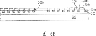
图6A至图6C是图5沿着III至III′的制作流程剖面示意图。6A to 6C are schematic cross-sectional views of the manufacturing process along III to III' in FIG. 5 .
图7A至图7C是图5的电感图形的俯视示意图,其中图7A是为电感图形204a,图7B是为电感图形210b,图7C是为电感图形214b。7A to 7C are schematic top views of the inductor pattern in FIG. 5 , wherein FIG. 7A is the inductor pattern 204 a , FIG. 7B is the
附图标号说明Explanation of reference numbers
100、200:衬底100, 200: Substrate
101、103、105:区域101, 103, 105: area
102、106、202、206:介电层102, 106, 202, 206: dielectric layer
104a、110a、112a、204a、210a、212a、214a:金属层104a, 110a, 112a, 204a, 210a, 212a, 214a: metal layers
104b、110b、112b、204b、210b、212b、214b:电感图形104b, 110b, 112b, 204b, 210b, 212b, 214b: inductance pattern
108a、108b、208a、208b:开口108a, 108b, 208a, 208b: openings
具体实施方式Detailed ways
第一实施例first embodiment
图1是表示依照本发明第一实施例的一种形成电感元件的结构的俯视示意图;图2A至图2C是表示图1中由I-I′的制作流程剖面示意图;图3A至图3C是表示图1中由II-II′的制造流程剖面示意图,其中在图1中所标示的101、103、105的区域是与图2A至图2C及图3A至图3C相互对应,而且区域105是表示区域101与区域103重叠的部分。并且于本实施例中,其所公开为一对称圆形螺旋式电感元件,并且该电感元件具有一交叉重叠区域。Fig. 1 is a schematic top view showing a structure for forming an inductance element according to the first embodiment of the present invention; Fig. 2A to Fig. 2C are schematic cross-sectional views showing the production process from I-I' in Fig. 1; Fig. 3A to Fig. 3C are representational diagrams 1, the schematic cross-sectional view of the manufacturing process from II-II', wherein the areas marked 101, 103, and 105 in Figure 1 correspond to Figures 2A to 2C and Figures 3A to 3C, and the
同时参照图1、图2A与图3A,电感元件的制作首先是提供衬底100,该衬底100上至少形成有介电层102,其材料例如是氧化硅、氮化硅、低介电常数材料等一般所熟知的介电材料,其形成方法例如先以化学气相沉积法,沉积介电层102于衬底100上,然后再以化学机械研磨法进行平坦化步骤。此处本技术领域的普通技术人员公知介电层102可为多数层的结构,并且在衬底100上与介电层102中可形成有多数的元件与金属内连线。Referring to Fig. 1, Fig. 2A and Fig. 3A at the same time, the manufacture of the inductance element is first to provide a
然后,于介电层102中同时形成图形化的金属层104a与电感图形104b,其中电感图形104b的俯视图如图4A所示,且金属层104a例如是衬底100上的多层金属内连线结构的最上层金属层,也即在进行金属内连线工序的过程中,可以在相同工序中形成电感图形104b。Then, a patterned metal layer 104a and an
此外,金属层104a与电感图形104b的材料例如是铜,其形成方法例如是以一般所熟知的金属镶嵌工序,首先于介电层102中形成图形化的开口(未图示),再将金属材料填入开口中以形成图形化的金属层104a与电感图形104b。In addition, the material of the metal layer 104a and the
接着,同时参照图1、图2B与图3B,于介电层102上形成图形化的介电层106,以覆盖金属层104a、电感图形104b与介电层102。此外,介电层106中更具有数个开口108a、108b,其中开口108a暴露出金属层104a,且开口108b暴露出电感图形104b。Next, referring to FIG. 1 , FIG. 2B and FIG. 3B , a patterned
除此之外,形成介电层106的方法例如是于介电层102上全面性地形成一层介电层(未表示),以覆盖金属层104a、电感图形104b与介电层102。之后进行化学机械研磨,以使该介电层全面平坦化。然后,利用公知技术的微影蚀刻工序来图形化该介电层,以定义出具有多数个开口108a、108b的介电层106。In addition, the method of forming the
另外,值得一提的是,为了在设计上避免电感元件短路,在图形化上述介电层形成开口108b时,于区域101与区域103并未形成开口108b,意即在后续工序中所形成的最上层的电感图形(未表示)不会通过中间层的电感图形(未表示)连接区域101与区域103中的电感图形104b,而除了区域101与区域103之外,开口108b的图形轨迹是与电感图形104b的图形相似。In addition, it is worth mentioning that, in order to avoid the short circuit of the inductance element in the design, when the above-mentioned dielectric layer is patterned to form the
之后,继续同时参照图1、图2B与图3B,于数个开口108a、108b中填入金属,以同时在开口108a中形成金属层110a,且于开口108b中形成电感图形110b。其中,所形成的金属层110a例如是作为金属插塞之用,且其是与金属层104a电连接。Afterwards, continue to refer to FIG. 1 , FIG. 2B and FIG. 3B at the same time, filling metal in
此外,形成电感图形110b与金属层110a的方式例如是于开口108a、108b中以及介电层106上形成一层金属层(未表示),其中金属材料例如是钨,且其形成方法例如是低压化学气相沉积法或是溅镀法。之后,再进行平坦化步骤,以移除开口108a、108b外的金属材料,而形成金属层110a与电感图形110b。因此,该电感图形110b是与金属层110a(例如:金属插塞)于同一步骤中同时形成。In addition, the way to form the
而且,上述所形成的电感图形110b的俯视图如图4B所示,其是与电感图形104b电连接,并且,除了在设计上避免电感元件短路,而在金属导线重叠区域附近(区域101、103、105)未形成电感图形110b之外,电感图形110b是具有与电感图形104b相似的图形。Moreover, the top view of the formed
继之,同时参照图1、图2C与图3C,于金属层110a上形成图形化的金属层112a,并且同时于电感图形110b上形成电感图形112b,其中金属层112a例如是作为金属焊垫之用,其是与金属层110a电连接。Next, referring to FIG. 1, FIG. 2C and FIG. 3C, a patterned metal layer 112a is formed on the metal layer 110a, and an
另外,金属层112a与电感图形112b的材料例如是铝,且其形成方法例如是于介电层106上形成全面性地金属层(未表示),其形成方式例如是物理气相沉积法。然后,利用公知微影蚀刻的技术,图形化该金属层以形成金属层112a与电感图形112b。因此,电感图形112b是与金属层112a(例如:金属焊垫)于同一步骤中同时形成。In addition, the material of the metal layer 112a and the
而且,上述所形成的电感图形112b的俯视图如图4C所示,其是与电感图形110b电连接,并且,除了在设计上避免电感元件短路,仅在区域105以及区域103处形成有电感图形112b之外,电感图形112b具有与电感图形110b、104b相似的图形。Moreover, the top view of the formed
值得一提的是,上述的多层的电感图形104b、110b与112b是构成一立体电感结构,其俯视图如图1所示,且该立体电感结构的交叉重叠区域(区域105)是由电感图形104b、介电层106与电感图形112b所构成,而且在该区域105的电感图形104b与电感图形112b并不借助电感图形110b连接,经由在立体电感结构的交叉重叠区域作上述设计,当电流沿着该立体电感结构流动时,在电流第一次流经交叉重叠区域时仅会沿着第一电感图形流动,并于电流第二次流经交叉重叠区域时仅沿着第三电感图形流动,因而能够避免电感图形于交叉重叠区域发生短路的问题。It is worth mentioning that the above-mentioned
此外,本发明并不限于上述的工序步骤,上述的金属层110a、112a,以及同时形成的电感图形110b、112b更可以用公知的双金属镶嵌工序来完成。In addition, the present invention is not limited to the above-mentioned process steps, and the above-mentioned metal layers 110a, 112a, and the
因此由上述工序可知,本发明利用多层的电感图形来增加电感元件的金属导线的厚度,如此可以降低电感元件的阻值,并增加其Q值,此外,在本发明的工序中,不需额外增加工序步骤就可完成电感元件的工序,因此本发明的方法可说是相当的简便。Therefore know by above-mentioned operation, the present invention utilizes the inductance pattern of multilayer to increase the thickness of the metal wire of inductance element, can reduce the resistance value of inductance element like this, and increase its Q value, in addition, in operation of the present invention, do not need The process of the inductance element can be completed by adding additional process steps, so the method of the present invention can be said to be quite simple.
尚且,在本发明的工序中,用以形成电感图形110b的开口108b,是能够与用以形成金属焊垫的插塞的开口108a一起形成,由于开口108a、108b是位于金属内连线结构的最上层,因此工序限制少,从而使得开口108b能够与电感图形104b具有相似的图形。Moreover, in the process of the present invention, the
以下对利用上述工序所制作出来的电感元件的结构加以说明,继续同时参照图1、图2C与图3C,其中图1是为本发明的电感元件的俯视示意图,图2C为图1沿着I至I′的剖面示意图,图3C为图1沿着II至II′的剖面示意图,其中在图1中所标示的101、103、105的区域是与图2C及图3C相互对应,而且区域105是表示区域101与区域103重叠的部分。The structure of the inductance element produced by the above process is described below, continue to refer to Fig. 1, Fig. 2C and Fig. 3C at the same time, wherein Fig. 1 is a schematic top view of the inductance element of the present invention, and Fig. 2C is a schematic diagram of Fig. 1 along I To the schematic cross-sectional view of I', Fig. 3C is a schematic cross-sectional view along II to II' of Fig. 1, wherein the areas marked 101, 103, 105 in Fig. 1 correspond to Fig. 2C and Fig. 3C, and the
本发明的电感元件的结构是架构于衬底100上,该衬底100上至少配置有介电层102。该电感元件结构包括三层电感图形104b、110b、112b。The structure of the inductance element of the present invention is built on the
其中,电感图形104b配置于介电层102上,该电感图形104b的俯视图如图4A所示,在介电层102上更配置有金属层104a,亦即金属层104a与电感图形104b配置于相同的膜层上,金属层104a例如是衬底100上的多层金属内连线结构的最上层金属层,且金属层104a与电感图形104b的材料例如是铜。值得一提的是,在区域103中,除了与区域101交叉重叠的区域105配置有电感图形104b外,其余的区域103并无电感图形104b的配置。Wherein, the
另外,电感图形110b配置于电感图形104b上,该电感图形110b的俯视图如图4B所示,除了交叉重叠区域之外,电感图形110b与电感图形104b具有相似的图形,且电感图形110b与电感图形104b电连接。此外,在金属层104a上更配置有金属层110a,亦即金属层110a与电感图形110b配置于相同的膜层上,该金属层110a例如是金属插塞,且金属层110a与电感图形110b的材料例如是钨。值得一提的是,在区域103与区域101中(包括交叉重叠的区域105),并无电感图形110b的配置。In addition, the
此外,电感图形112b配置于电感图形110b上,该电感图形112b的俯视图如图4C所示,除了交叉重叠区域之外,电感图形112b与电感图形110b、104b具有相似的图形,且电感图形112b与电感图形110b电连接。此外,在金属层110a上更配置有金属层112a,亦即金属层112a与电感图形112b配置于相同的膜层上,该金属层112a例如是金属焊垫114。值得一提的是,在区域101中,除了与区域103交叉重叠的区域105配置有电感图形112b外,其余的区域101并无电感图形112b的配置。In addition, the
另外,上述的三层的电感图形104b、110b、112b构成一立体电感结构,其俯视图如图1所示,且该立体电感结构的交叉重叠区域(区域105)是由电感图形104b、介电层106与电感图形112b所构成,而且在该区域105的电感图形104b与电感图形112b并不借助电感图形110b连接,以使电感图形于交叉重叠区域不会发生短路的问题。In addition, the three-
第二实施例second embodiment
图5是表示依照本发明第二实施例的一种电感元件的结构的俯视示意图;图6A至图6C是表示图5中由III-III′的制作流程剖面示意图。并且在本实施例中,其所公开为一同心螺旋式电感元件。5 is a schematic top view showing the structure of an inductance element according to the second embodiment of the present invention; FIGS. 6A to 6C are schematic cross-sectional views showing the manufacturing process from III-III' in FIG. 5 . And in this embodiment, it is disclosed as a concentric spiral inductance element.
同时参照图5与图6A,电感元件的制作首先是提供衬底200,接着在衬底200上至少形成有介电层202,其中该材料例如是氧化硅、氮化硅、低介电常数材料等一般所熟知的介电材料,其形成方法例如先以化学气相沉积法,沉积介电层202于衬底200上,然后再用化学机械研磨法进行平坦化步骤。此处本技术领域普通技术人员所公知介电层202可为多数层的结构,并且在衬底200上与介电层202中可形成有多数的元件与金属内连线。Referring to Fig. 5 and Fig. 6A at the same time, the manufacture of the inductance element is first to provide the
然后,于介电层202中同时形成图形化的金属层204a与电感图形204b ,其中电感图形204b的俯视图如图7A所示,且金属层204a例如是衬底200上的多层金属内连线结构的最上层金属层,也即在进行金属内连线工序的过程中,可以在相同工序中形成电感图形204b。Then, a patterned metal layer 204a and an
此外,金属层204a与电感图形204b的材料例如是铜,其形成方法例如是以一般所熟知的金属镶嵌工序,首先于介电层中形成图形化的开口(未图示),再将金属材料填入开口中以形成图形化的金属层204a与电感图形204b。In addition, the material of the metal layer 204a and the
接着,同时参照图5与图6B,于介电层202上形成图形化的介电层206,以覆盖金属层204a、电感图形204b与介电层202。此外,介电层206中更具有数个开口208a、208b,其中开口208a暴露出金属层204a,且开口208b暴露出电感图形204b,并且,开口208b的图形轨迹是与电感图形204b的图形相似,也即是沿着电感图形204b而形成螺旋状的开口208b。Next, referring to FIG. 5 and FIG. 6B simultaneously, a patterned
除此之外,形成介电层206的方法例如是于介电层202上全面性地形成一层介电层(未表示),以覆盖金属层、电感图形204与介电层202。之后进行化学机械研磨,以使该介电层全面平坦化。然后,利用公知技术的微影蚀刻工序来图形化该介电层,以定义出具有多数个开口208a、208b的介电层206。In addition, the method of forming the
之后,继续同时参照图5与图6C,在介电层206上形成填满开口208a、208b的金属层210a与电感图形210b,其中金属层210a是与金属层204a电连接,并可视为由开口中的金属层212a与介电层206上的金属层214a所构成,而开口208a中的金属层212a例如是可以作为金属插塞之用,介电层206上的金属层214a例如是可以作为金属焊垫之用。Afterwards, referring to FIG. 5 and FIG. 6C at the same time, a metal layer 210a and an
电感图形210b可视为单一电感图形,亦可以如同第一实施例,将之视为由开口208b中的电感图形212b与介电层206上的电感图形214b所构成。而且,由于开口208b具有与电感图形204b相似的图形,因此所形成的电感图形212b、214b也能够具有与电感图形204b相似的图形。The
此外,形成电感图形210b与金属层210a的方式,例如是于开口208a、208b中以及介电层206上形成一层金属层(未表示),其中金属材料例如是铝,且其形成方法例如是物理气相沉积法。之后,利用公知微影蚀刻的技术,图形化该金属层以形成金属层210a(212a、214a)与电感图形210b(212b、214b)。因此,电感图形210b是与金属层210a于同一步骤中同时形成。In addition, the way to form the
同样的,由于本发明是利用多层的电感图形来增加电感元件的金属导线的厚度,因此可以降低电感元件的阻值,并增加其Q值,此外,在本发明的工序中,不需额外增加工序步骤就可完成电感元件的工序,因此本发明的方法可说是相当的简便。Equally, because the present invention is to utilize multi-layer inductance pattern to increase the thickness of the metal wire of inductance element, therefore can reduce the resistance value of inductance element, and increase its Q value, in addition, in the process of the present invention, do not need additional The process of the inductance element can be completed by adding process steps, so the method of the present invention can be said to be quite simple.
尚且,在本发明的工序中,用以形成电感图形210b的开口208b,是能够与用以形成金属焊垫的插塞的开口208a一起形成,由于开口208a、208b是位于金属内连线结构的最上层,因此工序限制少,从而使得开口208b能够与电感图形204b具有相似的图形。Moreover, in the process of the present invention, the
再者,于本实施例中,由于金属层212a、214a与同时形成的电感图形212b、214b是可以于同一沉积、微影蚀刻步骤完成,因此与第一实施例相比是能够简化工序,尚且,对于电感图形212b、214b而言,由于是相同的材料,因此能够降低不同材料接触所造成的接触阻抗,增加其Q值。再者,对于电感图形212b而言,由于可以采用铝,与第一实施例采用钨相较之下,是能够降低接触阻抗,增加其Q值。Furthermore, in this embodiment, since the metal layers 212a, 214a and the
以下是对利用上述工序所制作出来的电感元件的结构加以说明,继续同时参照图5与图6C,其中图5是为本发明的电感元件的俯视示意图,图6C为图5沿着III至III′的剖面示意图。The following is a description of the structure of the inductance element produced by the above process. Continue to refer to FIG. 5 and FIG. 6C at the same time, wherein FIG. 5 is a schematic top view of the inductance element of the present invention, and FIG. ’Schematic cross-section.
本发明的电感元件的结构是架构于衬底200上,该衬底200上至少配置有介电层202。该电感元件结构包括电感图形204b、210b。The structure of the inductance element of the present invention is built on the
其中,电感图形204b配置于介电层202上,该电感图形204b的俯视图如图7A所示,并且在介电层202上更配置有金属层204a,也即金属层204a与电感图形204b配置于相同的膜层上,金属层204a例如是对底200上的多层金属内连线结构的最上层金属层,且金属层204a与电感图形204b的材料例如是铜。Wherein, the
电感图形210b配置于电感图形204b上,该电感图形210b的俯视图如图7C所示,且电感图形210b与电感图形204b电连接。此外,在金属层204a上更配置有金属层210a,且金属层210a配置于与电感图形210b相同的膜层上。于本实施例中,电感图形210b是可以视为由电感图形212b与电感图形214b所组成,依此观点,则电感图形212b的俯视是如图7B所示,且电感图形212b的俯视是如图7C所示。同样的,金属层210a是可以视为由金属层212a与金属层214a所组成,其中金属层212a例如是金属插塞,金属层214a例如是金属焊垫,并且金属层210a与电感图形210b的材料例如是铝。The
当然,上述的电感元件的形式并非限定于如图1所示的对称圆形螺旋式样或图5所示的同心圆形螺旋式样,其他例如对称方形螺旋样式或同心方形螺旋式样亦可利用本发明来加以完成。Of course, the form of the above-mentioned inductance element is not limited to the symmetrical circular spiral pattern shown in Figure 1 or the concentric circular spiral pattern shown in Figure 5, other such as symmetrical square spiral pattern or concentric square spiral pattern can also use the present invention to complete.
尚且,在第一实施例的对称圆形螺旋式电感元件中,其第一电感图形、第二电感图形、第三电感图形(最上层金属层、金属插塞、金属焊垫)是由不同的沉积工序所形成,然而本发明并不限定于此,第一实施例的电感元件亦可以如同第二实施例,使第二电感图形、第三电感图形(金属插塞、金属焊垫)于同一沉积、微影蚀刻步骤中完成,进一步来说,任意形式的电感元件都能够通过第一实施例或第二实施例所公开的工序以形成。Moreover, in the symmetrical circular spiral inductance element of the first embodiment, the first inductance pattern, the second inductance pattern, and the third inductance pattern (the uppermost metal layer, the metal plug, and the metal welding pad) are made of different The deposition process is formed, but the present invention is not limited thereto. The inductance element of the first embodiment can also be the same as the second embodiment, so that the second inductance pattern and the third inductance pattern (metal plugs, metal pads) are on the same The steps of deposition and lithographic etching are completed. Furthermore, any form of inductance element can be formed through the processes disclosed in the first embodiment or the second embodiment.
综上所述,由上述结构可知,本发明利用多层的电感图形来增加电感元件的金属导线的厚度,如此可以降低电感元件的阻值,更可以增加其Q值,进而提高电感元件的品质。In summary, it can be seen from the above structure that the present invention uses multi-layer inductance patterns to increase the thickness of the metal wire of the inductance element, so that the resistance value of the inductance element can be reduced, the Q value can be increased, and the quality of the inductance element can be improved. .
并且,由于本发明的多层电感元件的每一层具有相似的图形,因而使得整个电感元件结构具有均一的厚度,从而能够进一步有效增加其Q值。Moreover, since each layer of the multilayer inductive element of the present invention has a similar pattern, the entire inductive element structure has a uniform thickness, thereby further effectively increasing its Q value.
而且,由于该电感元件可与形成金属焊垫的工序一起制作,因此所形成的结构较公知更远离衬底,所以可以降低衬底对于电感元件所造成的导磁干扰,以提高晶片效能。Moreover, since the inductance element can be manufactured together with the process of forming metal pads, the formed structure is farther away from the substrate than conventionally known, so the magnetic interference caused by the substrate to the inductance element can be reduced to improve chip performance.
此外,由于本发明对应于金属插塞与金属焊垫部分的电感图形可于同一沉积、微影蚀刻步骤完成,因此工序得以简化。In addition, because the inductor pattern corresponding to the metal plug and the metal pad can be completed in the same deposition and photolithographic etching steps of the present invention, the process is simplified.
再者,由于对应于金属插塞或金属焊垫部分的电感图形是相同的材料,因此能够降低不同材料接触所造成的接触阻抗,从而增加电感元件的Q值。Furthermore, since the inductance pattern corresponding to the metal plug or the metal pad is made of the same material, the contact resistance caused by the contact of different materials can be reduced, thereby increasing the Q value of the inductance element.
虽然本发明已以数个较佳实施例公开如上,然而其并非用以限定本发明,任何本技术领域普通技术人员,在不脱离本发明的精神和范围内,当然可作些更动与润饰,因此本发明的保护范围当视以申请专利的要求书范围所界定的为准。Although the present invention has been disclosed above with several preferred embodiments, it is not intended to limit the present invention. Any person skilled in the art can certainly make some changes and modifications without departing from the spirit and scope of the present invention. , so the protection scope of the present invention should be regarded as defined by the claims of the patent application.
Claims (17)
Priority Applications (1)
| Application Number | Priority Date | Filing Date | Title |
|---|---|---|---|
| CNB2004100050416A CN100336169C (en) | 2004-02-16 | 2004-02-16 | Manufacturing method and structure of inductance element |
Applications Claiming Priority (1)
| Application Number | Priority Date | Filing Date | Title |
|---|---|---|---|
| CNB2004100050416A CN100336169C (en) | 2004-02-16 | 2004-02-16 | Manufacturing method and structure of inductance element |
Publications (2)
| Publication Number | Publication Date |
|---|---|
| CN1658370A CN1658370A (en) | 2005-08-24 |
| CN100336169C true CN100336169C (en) | 2007-09-05 |
Family
ID=35007742
Family Applications (1)
| Application Number | Title | Priority Date | Filing Date |
|---|---|---|---|
| CNB2004100050416A Expired - Lifetime CN100336169C (en) | 2004-02-16 | 2004-02-16 | Manufacturing method and structure of inductance element |
Country Status (1)
| Country | Link |
|---|---|
| CN (1) | CN100336169C (en) |
Families Citing this family (1)
| Publication number | Priority date | Publication date | Assignee | Title |
|---|---|---|---|---|
| CN103489852B (en) * | 2013-09-30 | 2016-01-27 | 江阴长电先进封装有限公司 | Packaging structure and packaging method of radio frequency inductor |
Citations (5)
| Publication number | Priority date | Publication date | Assignee | Title |
|---|---|---|---|---|
| US5446311A (en) * | 1994-09-16 | 1995-08-29 | International Business Machines Corporation | High-Q inductors in silicon technology without expensive metalization |
| JPH086514A (en) * | 1994-06-15 | 1996-01-12 | Yayoi Mitsuyoshi | Spring and poster pin with lead wire |
| US5656849A (en) * | 1995-09-22 | 1997-08-12 | International Business Machines Corporation | Two-level spiral inductor structure having a high inductance to area ratio |
| CN1378220A (en) * | 2001-03-29 | 2002-11-06 | 华邦电子股份有限公司 | Multilayer spiral inductor structure with high inductance and high quality factor |
| WO2003015110A1 (en) * | 2001-08-09 | 2003-02-20 | Koninklijke Philips Electronics N.V. | Planar inductive component and a planar transformer |
-
2004
- 2004-02-16 CN CNB2004100050416A patent/CN100336169C/en not_active Expired - Lifetime
Patent Citations (5)
| Publication number | Priority date | Publication date | Assignee | Title |
|---|---|---|---|---|
| JPH086514A (en) * | 1994-06-15 | 1996-01-12 | Yayoi Mitsuyoshi | Spring and poster pin with lead wire |
| US5446311A (en) * | 1994-09-16 | 1995-08-29 | International Business Machines Corporation | High-Q inductors in silicon technology without expensive metalization |
| US5656849A (en) * | 1995-09-22 | 1997-08-12 | International Business Machines Corporation | Two-level spiral inductor structure having a high inductance to area ratio |
| CN1378220A (en) * | 2001-03-29 | 2002-11-06 | 华邦电子股份有限公司 | Multilayer spiral inductor structure with high inductance and high quality factor |
| WO2003015110A1 (en) * | 2001-08-09 | 2003-02-20 | Koninklijke Philips Electronics N.V. | Planar inductive component and a planar transformer |
Also Published As
| Publication number | Publication date |
|---|---|
| CN1658370A (en) | 2005-08-24 |
Similar Documents
| Publication | Publication Date | Title |
|---|---|---|
| CN1260746C (en) | Film type common mode choke coil and manufacturing method thereof | |
| CN1231928C (en) | Common mode choke array | |
| CN1139122C (en) | Semiconductor device and manufacturing method thereof | |
| CN1624917A (en) | Inductor with high quality factor and manufacturing method thereof | |
| CN101047209A (en) | Capacitor structure and multilayer capacitor structure | |
| CN1601735A (en) | Semiconductor device and manufacturing method thereof | |
| CN1315745A (en) | Semiconductor device and manufacturing method thereof | |
| CN1779966A (en) | Semiconductor device | |
| CN1826670A (en) | Inductive and capacitive components for semiconductor technologies with minimum pattern density requirements | |
| CN1670945A (en) | Method for fabricating high performance copper laminate inductors | |
| CN1677661A (en) | Multilayer wiring structure with dummy patterns for improved surface flatness | |
| CN1798474A (en) | Printed circuit board having three-dimensional spiral inductor and method of fabricating same | |
| JP4772495B2 (en) | Inductor and method of forming inductor | |
| CN1581475A (en) | Wire-layingout structure | |
| CN1498443A (en) | Filter circuit apparatus and manufacturing method thereof | |
| CN1388977A (en) | Semiconductor inductor and methods for making the same | |
| CN1300850C (en) | Semiconductor device and method for fabricating the same | |
| CN1551313A (en) | Semiconductor device, stacked semiconductor device and manufacturing method thereof | |
| CN1870260A (en) | Bonding pad having metal pad in which slot is formed and mesh type via pattern | |
| CN1495898A (en) | Inductors for RF ICs | |
| CN1507055A (en) | IC Capacitors | |
| CN1502545A (en) | Microelectromechanical system encapsulated structure and manufacturing method thereof | |
| CN1297010C (en) | Semiconductor device with analog capacitor | |
| CN100346466C (en) | Semiconductor device and method of fabricating the same | |
| CN100338817C (en) | Substrate having microstrip line structure, semiconductor device having microstrip line structure, and manufacturing method of substrate having microstrip line structure |
Legal Events
| Date | Code | Title | Description |
|---|---|---|---|
| C06 | Publication | ||
| PB01 | Publication | ||
| C10 | Entry into substantive examination | ||
| SE01 | Entry into force of request for substantive examination | ||
| C14 | Grant of patent or utility model | ||
| GR01 | Patent grant | ||
| CX01 | Expiry of patent term | ||
| CX01 | Expiry of patent term |
Granted publication date: 20070905 |